

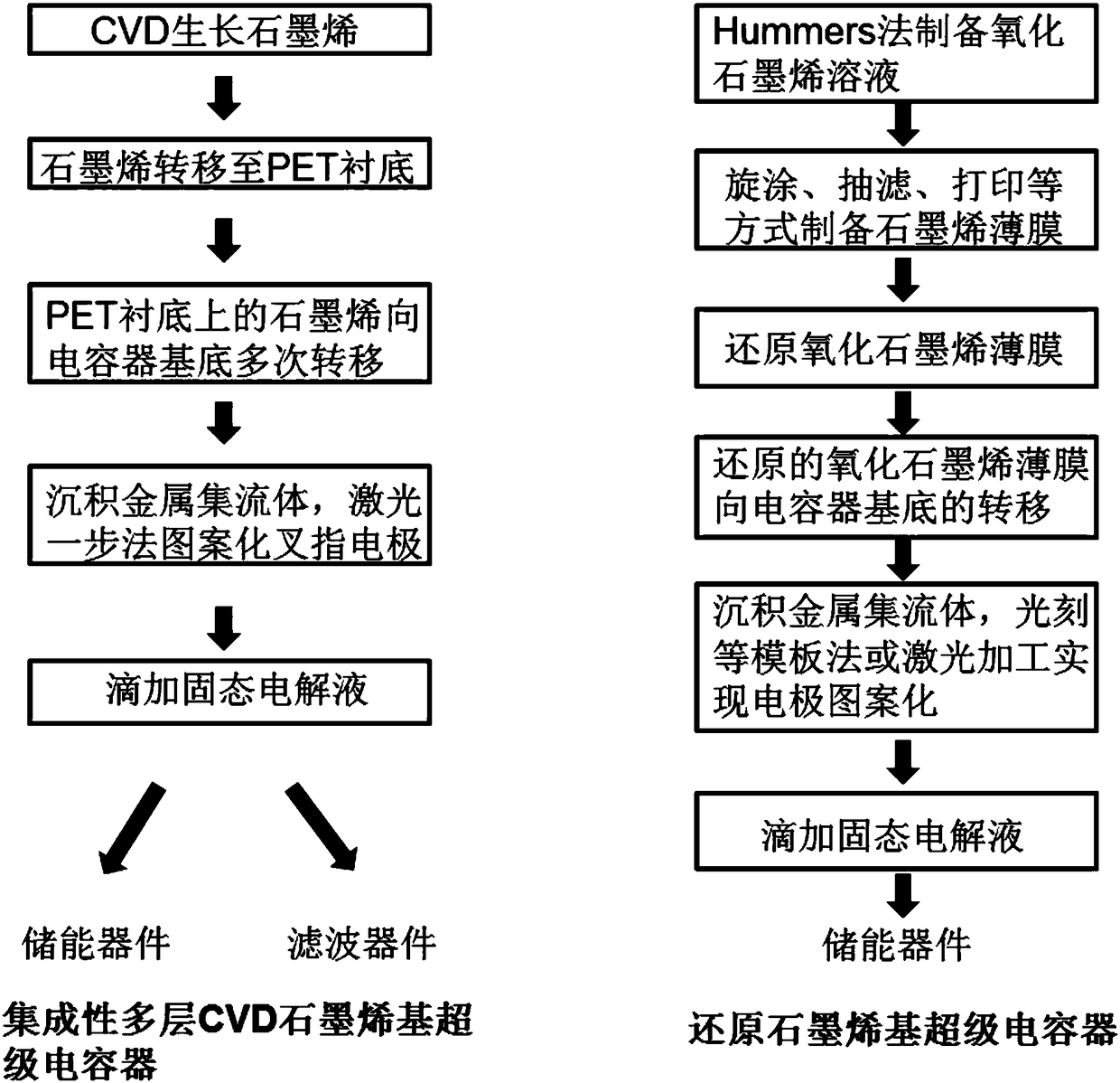
Graphene thin film electrode, preparation method thereof, graphene composite thin film interdigital electrode with conductive line formed on surface and capacitor
A technology of graphene film and film electrode, which is applied in the manufacture of hybrid capacitor electrodes, hybrid capacitor current collectors, and hybrid/electric double layer capacitors. Promotion and application, easy integration, and the effect of improving energy density
- Summary
- Abstract
- Description
- Claims
- Application Information
AI Technical Summary
Problems solved by technology
Method used
Image

Examples
preparation example Construction
[0092] The present invention also provides a kind of preparation method of graphene film electrode, comprises the following steps:
[0093] a) Composite a single-layer graphene sheet grown on a metal substrate on a flexible substrate, and remove the metal substrate by an etching solution to obtain an intermediate product;
[0094] b) transferring the single-layer graphene sheet on the intermediate product obtained in the above steps to the electrode substrate to obtain an electrode substrate composited with a graphene film;
[0095] Said transfer includes a single transfer or multiple transfers;
[0096] c) Depositing a metal film on the graphene film of the electrode substrate compounded with the graphene film obtained in the above steps to obtain a graphene film electrode.
[0097] The selection, combination and preferred range of materials in the preparation method of the graphene thin film electrode in the present invention preferably correspond to the selection, combinat...
Embodiment 1
[0128] a) High-quality graphene was grown on copper foil (thickness 20 μm, area the size of a standard A4 paper) by chemical vapor deposition, the growth temperature was 1000 °C, the growth time was 10 min, CH 4 Gas flow rate is 10sccm, hydrogen 10sccm;
[0129] b) The copper foil grown with graphene is tightly attached to the PET substrate (Cu / PET) by rolling, and the Cu / PET film is placed in 0.5M (NH 4 )S 2 o 8 In the etching solution, the etching time is 2 to 4 hours to completely etch Cu;
[0130] c) Lay the resulting flexible PET / graphene substrate to the supercapacitor PET substrate (125 μm), or to the PTFE film substrate, and after keeping it at 90°C for 20 minutes, slowly peel off the PET substrate to realize graphene Transfer to PET substrate / PTFE substrate;
[0131] d) Repeat step c) 3 times to obtain a 3-layer graphene film conductive film electrode, the size of which is the size of a standard A4 paper.
Embodiment 2
[0133] a) High-quality graphene was grown on copper foil (thickness 20 μm, area the size of a standard A4 paper) by chemical vapor deposition, the growth temperature was 1030 °C, and the growth time was 20 min; CH 4 The gas flow rate is 3 sccm, and the hydrogen gas is 10 sccm;
[0134] b) The graphene-grown copper foil is tightly attached to the PET substrate (Cu / PET) by rolling, and the Cu / PET film is placed in 0.5M FeCl 3 In the etching solution, the etching time is 1 to 2 hours to completely etch Cu;
[0135] c) cutting the resulting flexible PET / graphene substrate into a size of 25 cm 2 A small piece; and bonded to the supercapacitor PET substrate (50 μm), after maintaining at 100 ° C for 20 minutes, slowly peel off the PET substrate, so as to realize the transfer of graphene to the PET substrate;
[0136] d) Repeat step c) 6 times to obtain a 6-layer graphene film conductive film electrode with a size of 25cm 2 .
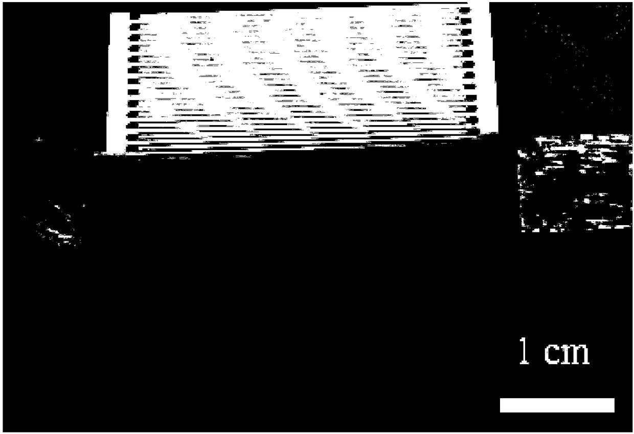
[0137] see figure 2 , figure 2 It is the physical...
PUM
| Property | Measurement | Unit |
|---|---|---|
| Thickness | aaaaa | aaaaa |
| Area | aaaaa | aaaaa |
| Layer spacing | aaaaa | aaaaa |
Abstract
Description
Claims
Application Information