GaN heterojunction longitudinal power device
A power device and heterojunction technology, applied in semiconductor devices, electrical components, circuits, etc., can solve the problems of not being able to fully utilize the advantages of GaN material withstand voltage, reduced reliability, and injection damage
Inactive Publication Date: 2018-09-28
UNIV OF ELECTRONIC SCI & TECH OF CHINA
View PDF7 Cites 6 Cited by
- Summary
- Abstract
- Description
- Claims
- Application Information
AI Technical Summary
Problems solved by technology
[0006] 2. In recent years, the research work of enhanced GaN HEMT has made great progress, but the threshold voltage of enhanced GaN HEMT is relatively low (mostly less than 1V), and the performance is obviously worse than that of depletion-type HEMT.
[0008] (1) Reducing the Al composition or growing a thin barrier layer reduces the 2DEG concentration in the channel, but increases the parasitic resistance and on-state resistance of the AlGaN / GaN HEMT, so the Al composition and barrier layer thickness can only be limited reduced within the range, the threshold voltages are relatively low
[0009] (2) Growth of p-cap capping layer to achieve enhanced HEMT, but the capping layer weakens the control of the gate to the channel, reduces the transconductance of the device, which is not good for high-frequency work, and P-cap technology will introduce P-N junction When the device is working, a large number of holes will be injected into the channel, which will generate a large gate current, resulting in a series of problems such as threshold voltage hysteresis and reliability reduction.
[0010] (3) Recessed gate etching can effectively deplete the 2DEG concentration under the gate, but recessed gate etching requires precise control of the etching depth and will introduce serious etching damage
[0011] (4) F-based plasma treatment is a very promising method to realize enhanced HEMT, but it will introduce injection damage, threshold voltage hysteresis, and high-voltage operation stability problems
However, this technology cannot completely deplete the two-dimensional electron gas in the channel, and cannot give full play to the withstand voltage advantages of GaN materials. At the same time, the deep energy level traps introduced by impurities such as carbon and iron will cause such as increased on-resistance, decreased output current, Negative effects such as current collapse effect and decreased reaction speed
Method used
View moreImage
Smart ImageViewing Examples

Examples
Embodiment Construction
[0038] The solution of the present invention has been described in detail in the part of the summary of the invention, and will not be repeated here.
Login to View More PUM
| Property | Measurement | Unit |
|---|---|---|
| Length | aaaaa | aaaaa |
| Doping concentration | aaaaa | aaaaa |
Abstract
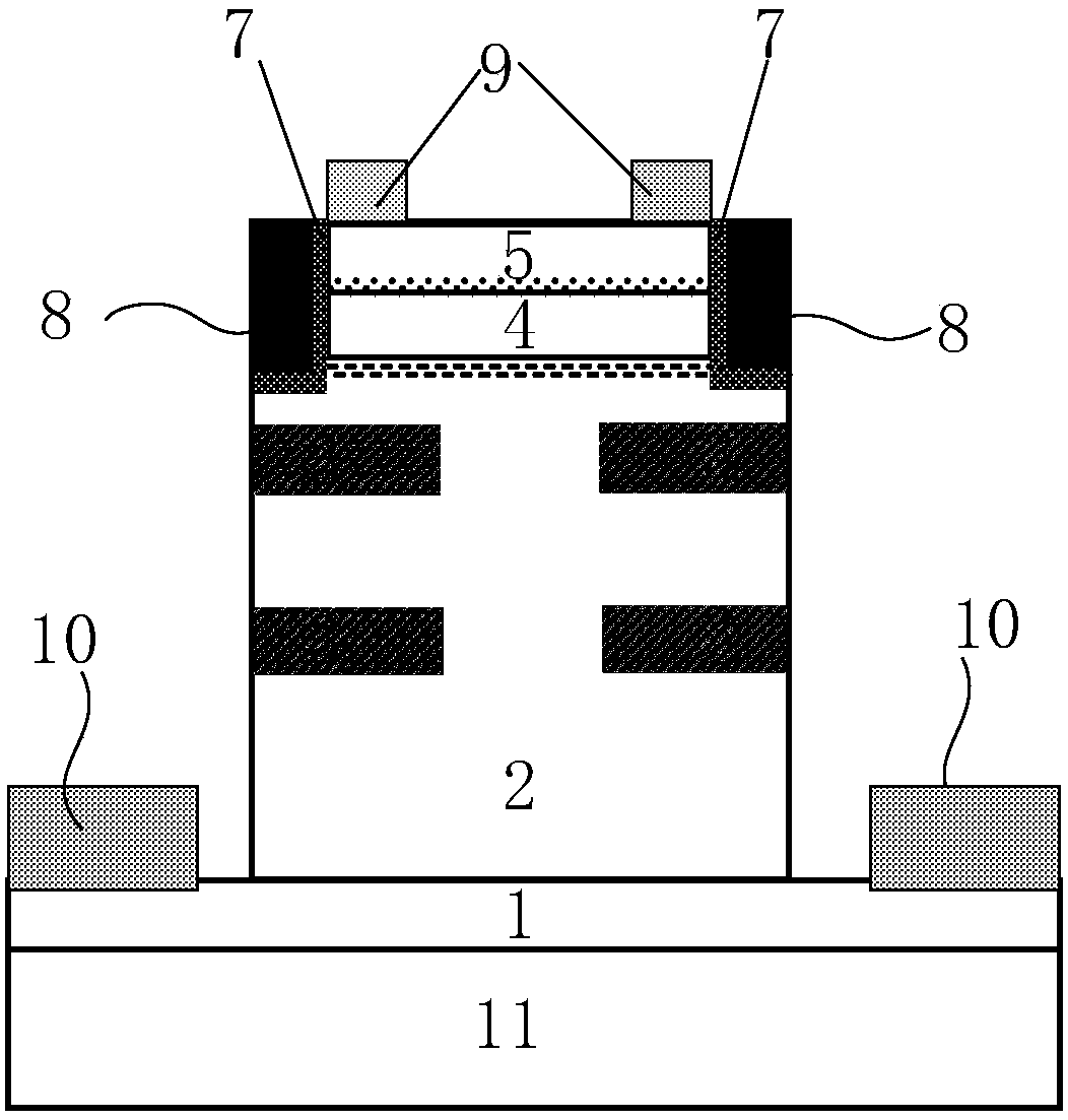
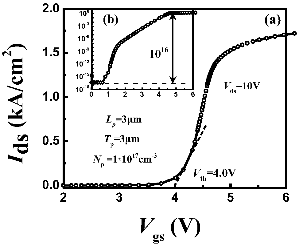
The invention discloses a GaN heterojunction longitudinal power device. According to the GaN heterojunction longitudinal power device disclosed by the invention, source electrode electrons are prevented from being injected into a two-dimensional electron gas channel through a longitudinal grid control channel by using a two-dimensional hole gas, a device enhancement type is achieved, and the longitudinal device realizes low on resistance and large saturation current by using the two-dimensional electron gas channel with a high migration rate; meanwhile, a reverse biased PN junction is importedto a GaN drift region of a floating P-type GaN buried layer, an exhaustion region of the reverse biased PN junction continuously expands when the reverse biased PN junction withstands a reverse withstand voltage, so that the electric field in the device is uniformly distributed, so that the maximum peak electric field in the device is effectively reduced. By adjusting the doping concentration, the thickness and the length of P-GaN type drift region, the P-GaN drift region is almost simultaneously depleted with the N-type drift region, so that the exhaustion region between the reverse biased PN junctions of the P-GaN type drift region and the N type type drift region is expanded to a larger exhaustion region to withstand the reverse voltage, the advantages of a large forbidden band width and a high withstand voltage of a GaN body material are fully played, and the reliability and the stability of a power electronic circuit system are improved.
Description
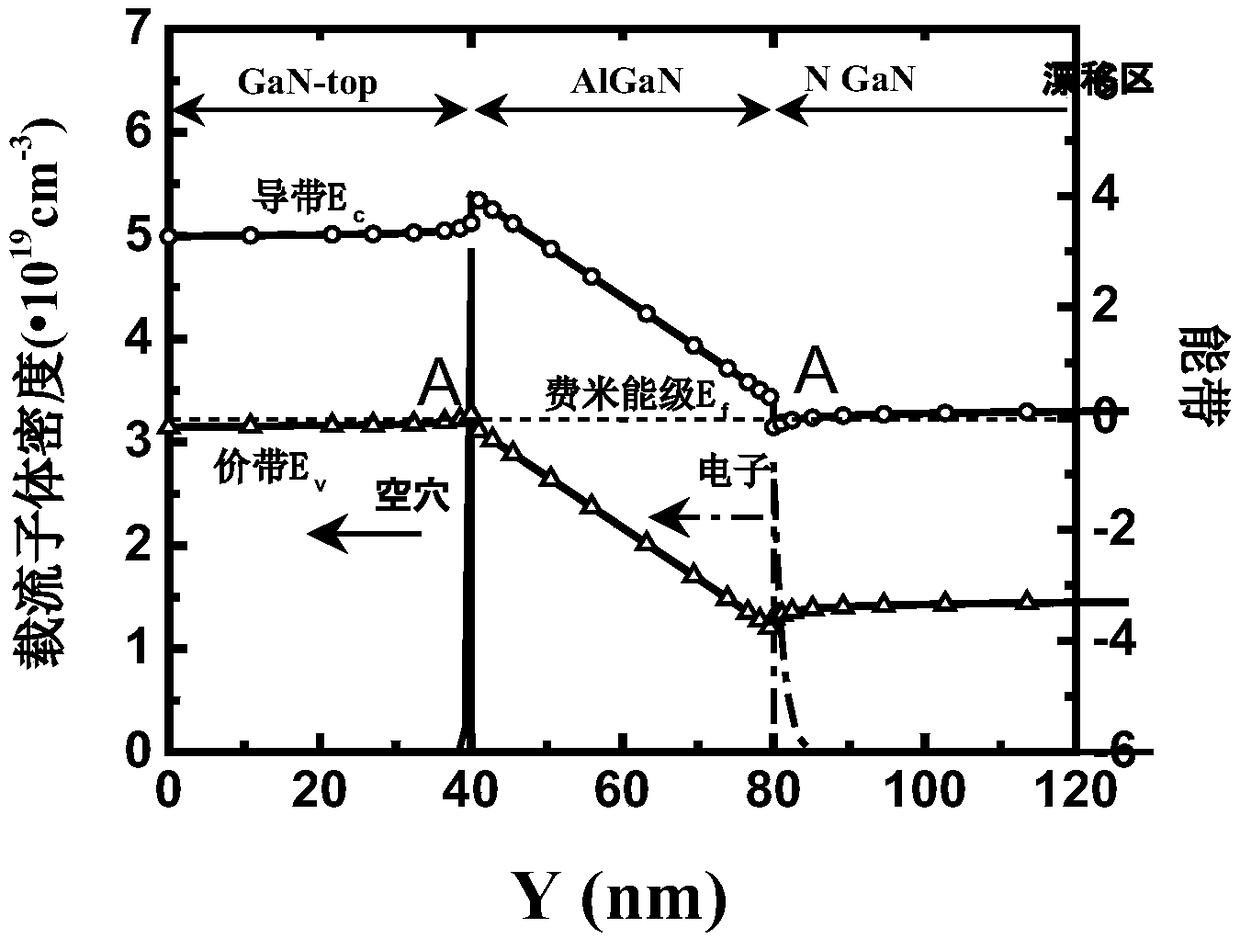
technical field [0001] The invention belongs to the technical field of power semiconductors, and relates to a GaN heterojunction vertical power device. Background technique [0002] Due to the limitations of the first two generations of semiconductor materials represented by Si and GaAs, the third generation of wide bandgap semiconductor materials has been developed rapidly because of its excellent performance. Gallium nitride (GaN) material is one of the cores of the third-generation semiconductor materials. Compared with Si, GaAs and silicon carbide (SiC), the special feature is that it has a polarization effect. Due to the polarization effect of the AlGaN / GaN heterojunction, a two-dimensional electron gas conduction channel with high concentration and high electron mobility is generated at the heterojunction interface close to the GaN side, which makes the AlGaN / GaN HEMT device have small on-resistance and fast switching speed. The characteristics of fast and high forwar...
Claims
Login to View More Application Information
Patent Timeline
 IPC IPC(8): H01L29/778H01L29/06
CPCH01L29/0615H01L29/0661H01L29/7783
Inventor 周琦魏东邓操董长旭黄芃陈万军张波
Owner UNIV OF ELECTRONIC SCI & TECH OF CHINA
Features
- R&D
- Intellectual Property
- Life Sciences
- Materials
- Tech Scout
- Unparalleled Data Quality
- Higher Quality Content
- 60% Fewer Hallucinations
Learn More Browse by: Latest US Patents, China's latest patents, Technical Efficacy Thesaurus, Application Domain, Technology Topic, Popular Technical Reports.
© 2025 PatSnap. All rights reserved.Legal|Privacy policy|Modern Slavery Act Transparency Statement|Sitemap|About US| Contact US: help@patsnap.com