High-mobility n-type nano diamond film of crystalline grain closely-packed structure and preparation method of high-mobility n-type nano diamond film

A nano-diamond, high-mobility technology, applied in the field of high-mobility n-type nano-diamond films and preparation, can solve problems such as hindering the electrical properties of the films, and achieve the effects of easy operation and simple method

Active Publication Date: 2018-10-16
ZHEJIANG UNIV OF TECH
View PDF2 Cites 4 Cited by
  • Summary
  • Abstract
  • Description
  • Claims
  • Application Information

AI Technical Summary

Problems solved by technology

At the same time, in the existing methods, ion implantation is mainly performed on ordinary nano-diamond films. This type of nano-diamond film is composed of nano-diamond grains and obvious amorphous carbon grain boundaries. A large number of amorphous carbon grain boundaries hinder the electrical properties of the film. Further performance improvements

Method used


Image

  • High-mobility n-type nano diamond film of crystalline grain closely-packed structure and preparation method of high-mobility n-type nano diamond film
  • High-mobility n-type nano diamond film of crystalline grain closely-packed structure and preparation method of high-mobility n-type nano diamond film
  • High-mobility n-type nano diamond film of crystalline grain closely-packed structure and preparation method of high-mobility n-type nano diamond film

Examples


Embodiment 1

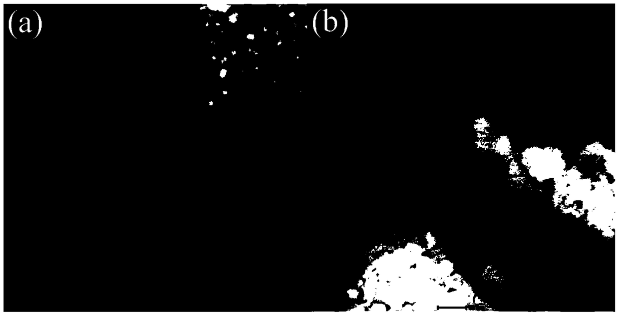
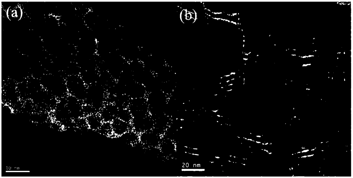
[0027]The monocrystalline silicon wafer was ultrasonically oscillated with a mixture of diamond micropowder (0.1 g) and acetone (50 ml), and the oscillating time was 30 min. The shaken silicon wafer was ultrasonically cleaned twice with acetone reagent, each time for 2 min, and the dried silicon wafer was used as the substrate for the growth of the nanocrystalline grain close-packed diamond film. Using hot wire chemical vapor deposition method (chemical vapor deposition equipment purchased from Shanghai Jiaoyou Diamond Coating Co., Ltd., equipment model: JUHFCVD001), using acetone at 0°C as the carbon source, and using hydrogen bubbling to bring acetone into the reaction chamber , the flow rate is 80sccm, the additional hydrogen flow rate is 200sccm, the temperature of the reaction chamber is controlled within the range of 500-600°C, the power of the hot wire is 2200W, the bias voltage is turned off during the growth process, the growth time of the nano-diamond film is 50 minut...

Embodiment 2

[0033] The monocrystalline silicon wafer was ultrasonically oscillated with a mixture of diamond micropowder (0.1 g) and acetone (50 ml), and the oscillating time was 30 min. The shaken silicon wafer was ultrasonically cleaned twice with a clean acetone reagent, each time for 2 min, and the dried silicon wafer was used as the substrate for the growth of the nanocrystal grain close-packed diamond film. Using hot wire chemical vapor deposition method (chemical vapor deposition equipment purchased from Shanghai Jiaoyou Diamond Coating Co., Ltd., equipment model: JUHFCVD001), using acetone at 0°C as the carbon source, and using hydrogen bubbling to bring acetone into the reaction chamber , the flow rate is 90 sccm, the additional flow rate of hydrogen gas is 200 sccm, the temperature of the reaction chamber is controlled in the range of 500-600 ° C, the power of the hot wire is 2400 W, the bias voltage is turned off during the growth process, and the growth time of the nano-diamond...

Embodiment 3

[0039] The monocrystalline silicon wafer was ultrasonically oscillated with a mixture of diamond micropowder (0.1 g) and acetone (50 ml), and the oscillating time was 30 min. The shaken silicon wafer was ultrasonically cleaned twice with acetone reagent, each time for 2 min, and the dried silicon wafer was used as the substrate for the growth of the nanocrystalline grain close-packed diamond film. Using hot wire chemical vapor deposition method (chemical vapor deposition equipment purchased from Shanghai Jiaoyou Diamond Coating Co., Ltd., equipment model: JUHFCVD001), using acetone at 0°C as the carbon source, and using hydrogen bubbling to bring acetone into the reaction chamber , the flow rate is 80sccm, the additional hydrogen flow rate is 200sccm, the temperature of the reaction chamber is controlled within the range of 500-600°C, the power of the hot wire is 2200W, the bias voltage is turned off during the growth process, the growth time of the nano-diamond film is 50 minu...


PUM

PropertyMeasurementUnit
thicknessaaaaaaaaaa
particle sizeaaaaaaaaaa
thicknessaaaaaaaaaa

Abstract

The invention discloses a high-mobility n-type nano diamond film of a novel micro-structure and a preparation method of the high-mobility n-type nano diamond film. A hot filament chemical vapor deposition (HFCVD) method is adopted, and the nano diamond film is prepared on a monocrystalline silicon substrate. Acetone serves as a carbon source, the carbon source is brought into a reaction chamber cavity body in a hydrogen bubbling manner, the growth time is about 40-60 minutes, the nano diamond film with the thickness being about 1-3 microns is prepared, the crystalline grain size is 10-30 nm, and the content of the amorphous carbon grain boundary in the film is quite small. The crystalline grain closely-packed nano diamond film is subjected to injection of sulfur ions and oxygen ions, an injected sample is then subjected to low-vacuum annealing, and the n-type nano diamond film with the mobility universally reaching 400 cm<2> / V.s or above can be obtained. The high-mobility n-type nano diamond film has quite great significance and value for achieving the goal of applying the diamond film to the fields such as semiconductor devices, photoelectron and field emission displays.

Description

technical field [0001] The invention relates to a high-mobility n-type nano-diamond thin film with a crystal grain close-packed structure and a preparation method. Background technique [0002] Diamond has a wide band gap, which makes it a new generation of semiconductor materials after silicon, germanium and other materials, and has broad application prospects in high-tech fields such as machinery, optoelectronics, electrochemistry, and semiconductors. However, diamond has not been applied in the microelectronics industry at present. The key reason is that it is difficult to prepare n-type diamond films with low resistivity and high mobility, which makes it difficult to make prototype devices such as pn junctions. The successful preparation of n-type diamond films with high conductivity and the realization of the application of diamond in the microelectronics industry may lead to a revolution in the electronics industry, which has extremely important theoretical and applica...

Claims


Application Information

Patent Timeline
Patent Type & Authority Applications(China)
IPC IPC(8): C23C16/27C23C16/56C23C14/48
CPCC23C14/48C23C16/271C23C16/56
Inventor 胡晓君陈成克徐辉刘建军梅盈爽樊冬
Owner ZHEJIANG UNIV OF TECH
Why Eureka
Try Eureka