Semiconductor device and method of forming the same

A semiconductor and device technology, applied in the field of semiconductor devices and their formation, can solve the problems of high subthreshold slope of TFET and deterioration of device subthreshold characteristics, and achieve the effect of reducing subthreshold slope and increasing current

Active Publication Date: 2022-04-15
SEMICON MFG INT (SHANGHAI) CORP +1
View PDF0 Cites 0 Cited by
  • Summary
  • Abstract
  • Description
  • Claims
  • Application Information

AI Technical Summary

Problems solved by technology

[0004] However, since the subthreshold slope of a TFET is a strong function of the gate voltage, the subthreshold characteristics of the device tend to deteriorate as the gate voltage increases
Therefore, the TFET formed by the prior art still has the problem of high subthreshold slope

Method used


Image

  • Semiconductor device and method of forming the same
  • Semiconductor device and method of forming the same
  • Semiconductor device and method of forming the same

Examples


Embodiment Construction

[0032] There are many problems in the semiconductor devices in the prior art, for example, high sub-threshold slope and high energy consumption.

[0033] Combining with the semiconductor structure of the prior art, the reason why the sub-threshold slope of the semiconductor device of the prior art is relatively high and the energy consumption is large is analyzed:

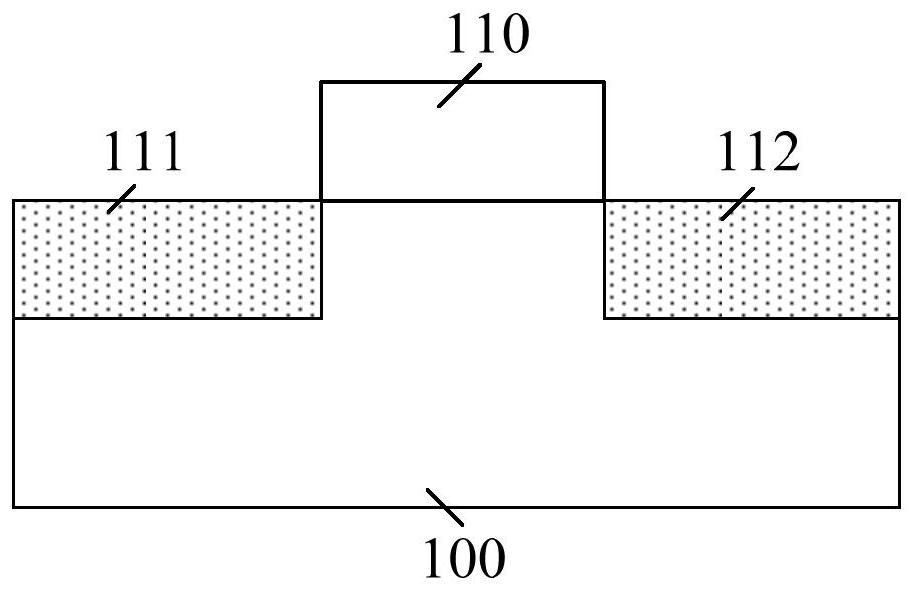
[0034] figure 1 It is a schematic diagram of the structure of a semiconductor device.

[0035] Please refer to figure 1 , the semiconductor device includes: a semiconductor substrate 100; a gate structure 110 located on the semiconductor substrate 100; a source region 111 and a drain region 112 respectively located in the semiconductor substrate 100 on both sides of the gate structure 110, The source region 111 has first dopant ions, and the drain region 112 has second dopant ions, and the second dopant ions have a conductivity type opposite to that of the first dopant ions.

[0036] Wherein, the semiconductor s...


PUM

PropertyMeasurementUnit
thicknessaaaaaaaaaa
thicknessaaaaaaaaaa

Abstract

The present invention provides a semiconductor device and a method for forming the same, wherein the method includes: forming a semiconductor substrate, the semiconductor substrate including a gate region and a first region and a second region respectively located on both sides of the gate region, There is an epitaxial layer in the semiconductor substrate in the first region, and the energy gap of the epitaxial layer is smaller than the energy gap of the semiconductor substrate; a first doped region is formed in the epitaxial layer in the first region, and the first There are first doping ions in the doping region; a gate structure is formed on the semiconductor substrate in the gate region; a second doping region is formed in the semiconductor substrate in the second region, and the second doping region There are second dopant ions in which the conductivity type of the second dopant ions is opposite to that of the first dopant ions. If the bandgap of the epitaxial layer is smaller than that of the semiconductor substrate, the barrier width on the contact surface between the first doped region and the channel region will be smaller. Therefore, the forming method can reduce the Formation of subthreshold slopes for semiconductor devices.

Description

technical field [0001] The invention relates to the technical field of semiconductor manufacturing, in particular to a semiconductor device and a forming method thereof. Background technique [0002] With the improvement of the integration level of semiconductor devices, the critical dimensions of transistors are continuously reduced, and the reduction of critical dimensions means that more transistors can be arranged on a chip. However, with the sharp reduction of transistor size, CMOS field effect transistors face great challenges, such as increased short channel effects, increased leakage current, and subthreshold slope with a limit of 60mV / dec at room temperature. [0003] In order to adapt to the reduction of transistor size, suppress the short channel effect, and reduce the subthreshold slope, TFET (tunnelfield-effect transistor, tunneling field-effect transistor) emerged as the times require. TFET is a metal oxide semiconductor gated PIN diode. TFET mainly uses the ...

Claims


Application Information

Patent Timeline
Patent Type & Authority Patents(China)
IPC IPC(8): H01L29/739H01L21/331
CPCH01L29/66356H01L29/7391
Inventor 陈卓凡
Owner SEMICON MFG INT (SHANGHAI) CORP
Why Eureka
Try Eureka