Silicon-based graphene photoelectric detector

A photodetector, graphene technology, applied in the optical field, can solve the problems of low detector responsivity, limited detector bandwidth, high extra light, etc., to achieve the effect of realizing broadband response, avoiding resonance effect, and improving responsivity

Active Publication Date: 2018-11-27
HUAZHONG UNIV OF SCI & TECH
View PDF7 Cites 3 Cited by
  • Summary
  • Abstract
  • Description
  • Claims
  • Application Information

AI Technical Summary

Problems solved by technology

[0004] In view of the defects of the prior art, the purpose of the present invention is to solve the problem of low detector responsivity due to the limited interaction between the light field and graphene in ordinary sili

Method used


Image

  • Silicon-based graphene photoelectric detector
  • Silicon-based graphene photoelectric detector
  • Silicon-based graphene photoelectric detector

Examples


Embodiment Construction

[0020] In order to make the object, technical solution and advantages of the present invention clearer, the present invention will be further described in detail below in conjunction with the accompanying drawings and embodiments. It should be understood that the specific embodiments described here are only used to explain the present invention, not to limit the present invention.

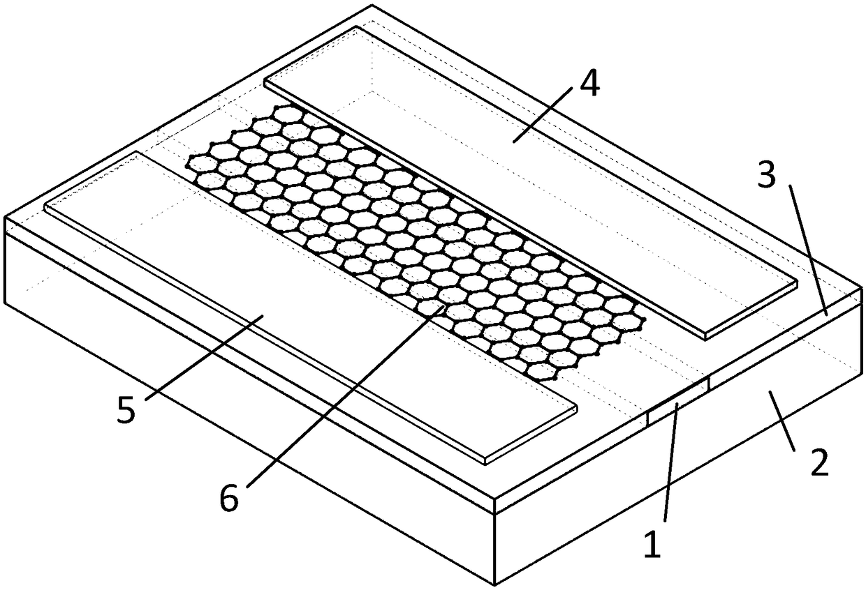
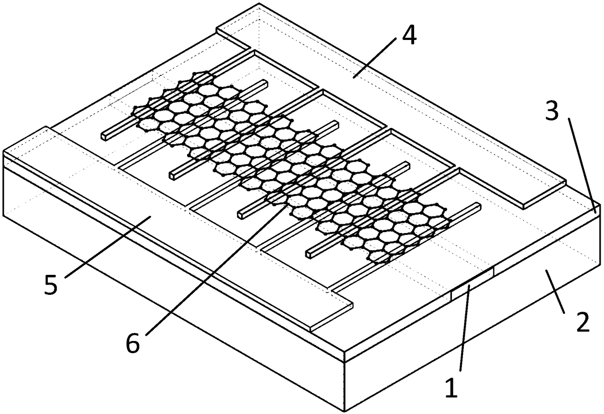
[0021] figure 1 It is a schematic structural diagram of a common silicon-based graphene photodetector in the prior art. like figure 1 As shown, a common silicon-based graphene photodetector includes a silicon waveguide 1 , an oxide substrate layer 2 , an oxide cladding layer 3 , a first metal electrode 4 , a second metal electrode 5 and graphene 6 .

[0022] The silicon waveguide 1 acts as a light guide, and it is generally a rectangular silicon waveguide with a width set to 500nm, which can support single-mode transmission of 1550nm light.

[0023] The oxide substrate layer 2 and the oxide clad...


PUM


Abstract

The invention discloses a silicon-based graphene photoelectric detector. The silicon-based graphene photoelectric detector comprises a silicon waveguide, an oxide substrate layer, an oxide cladding layer and graphene, and further comprises sub-wavelength metal electrodes composed of a first metal electrode and a second metal electrode, which are symmetrically arranged, wherein the sub-wavelength metal electrodes are crossly arrayed above the silicon waveguide by adopting two different types of metal. According to the silicon-based graphene photoelectric detector disclosed by the invention, twodifferent types of the metal are in contact with graphene to generate doping of different concentrations or types, so that electric potential difference is introduced between the sub-wavelength metalelectrodes and is used for driving a photon-generated carrier to flow toward the two electrodes. According to the silicon-based graphene photoelectric detector disclosed by the invention, the contactarea between the electrodes and the graphene is enlarged through a crossed arrangement structure of the electrodes, and the absorption efficiency of the carrier is improved; the graphene is laminatedon upper surfaces of the sub-wavelength metal electrodes and the sub-wavelength metal electrodes are used for carrying out optical field regulation and control on a transverse magnetic (TM) model transmitted in the silicon waveguide to increase an electric field component in a direction parallel to the graphene, so that the interaction effect between an optical field and the graphene is enhancedand the responsiveness of the detector is improved.

Description

technical field [0001] The invention belongs to the field of optics, and more specifically relates to a silicon-based graphene photodetector. Background technique [0002] Compared with traditional optical platforms, silicon-based photonics has many advantages, such as low power consumption, large bandwidth, small size, compatibility with traditional microelectronics production processes (ie CMOS processes), etc., and has been developed to solve the next generation of high-speed optical An important discipline in communication and optical interconnection. As a basic device on a silicon-based platform, photodetectors have received extensive attention and research. Common on-chip detectors include III-V detectors and germanium (Ge) detectors, but III-V detectors are not compatible with traditional CMOS processes, resulting in high manufacturing costs, and Ge detectors due to their electrical properties The disadvantage is that the bandwidth is difficult to exceed 100GHz. In...

Claims


Application Information

Patent Timeline
IPC IPC(8): H01L31/09H01L31/108
CPCH01L31/09H01L31/108
Inventor 余宇左炎张新亮
Owner HUAZHONG UNIV OF SCI & TECH
Why Eureka
Try Eureka