Large-area and graphical transition metal sulfide thin film preparation methods

A transition metal and transition group metal technology, which is applied in the field of preparation of large-area and patterned transition metal sulfide thin films, can solve the problems of inability to realize patterned thin film preparation, etc. Effect

Pending Publication Date: 2018-11-30
CHONGQING UNIVERSITY OF SCIENCE AND TECHNOLOGY
View PDF4 Cites 14 Cited by
  • Summary
  • Abstract
  • Description
  • Claims
  • Application Information

AI Technical Summary

Problems solved by technology

[0003] At present, the preparation of transition metal sulfide thin films is mainly based on mechanical exfoliation, and the mechanical exfoliation method can only obtain two-dimensional thin films with a small area, and cannot realize the preparation of patterned thin films.
[0004] Due to the limitations of the current preparation technology, transition metal sulfide films can only be obtained in a small area, which can only be limited to academic research. In view of this, the large-area preparation of two-dimensional transition metal sulfide materials is an urgent need in this technical field. question

Method used


Image

  • Large-area and graphical transition metal sulfide thin film preparation methods
  • Large-area and graphical transition metal sulfide thin film preparation methods
  • Large-area and graphical transition metal sulfide thin film preparation methods

Examples


Embodiment 1

[0028] Preparation of a large-area platinum diselenide thin film:

[0029] 1) Select a silicon wafer grown by thermal oxidation of 300nm silicon dioxide, with an area of ​​3 square centimeters, and clean it;

[0030] 2) Deposition of platinum metal film: use magnetron sputtering to grow platinum with a thickness of 3nm on the cleaned substrate;

[0031] 3) Synthesis in a chemical vapor deposition system: Place the selenium powder upstream of the platinum metal film, and set its heating temperature to 220°C, so that the selenium powder is in a molten state, and then make the lining with the platinum metal film grow The bottom is placed at 400°C, H 2 Set as 10SCCM, Ar as 100SCCM flow rate, air pressure as 70Pa, in H 2 Under the action of Ar and Ar, the selenium atoms are transported to the platinum atoms and combined to form platinum diselenide. The synthesis time is 60 minutes. During the synthesis process, the vacuum pump is used to keep the cavity in a low pressure state. A...

Embodiment 2

[0033] The difference from Example 1 is that step 2) deposition of platinum metal film: use magnetron sputtering to grow platinum with a thickness of 1 nm on the cleaned substrate;

[0034] The platinum diselenide thin film prepared in embodiment 1 is characterized,

[0035] (1) Characterization of the morphology of platinum diselenide

[0036] refer to figure 1 , it can be seen that the platinum diselenide prepared in Example 1 presents the characteristics of large area, uniformity and continuity, which meets the needs of large area preparation.

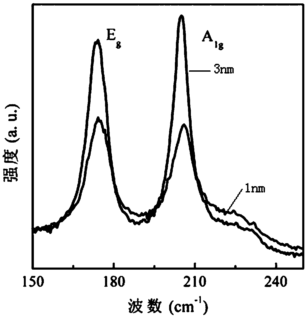
[0037] (2) Raman spectrum characterization of platinum diselenide

[0038] Platinum diselenide is a kind of transition metal sulfide, and the layers are combined by weak van der Waals force, so in addition to the lattice vibration in the plane, there is also the interaction between the planes, Raman spectroscopy as The means of detecting phonon vibration characteristics can also be used to characterize platinum diselenide and obt...

Embodiment 3

[0042] The method that present embodiment prepares molybdenum disulfide comprises the steps:

[0043] (1) Gallium nitride wafer is selected as the substrate material, and gallium nitride is cleaned.

[0044] (2) Deposition of molybdenum metal film: Molybdenum with a thickness of 10 nm was grown on the cleaned substrate by magnetron sputtering.

[0045] (3) Synthesis in chemical vapor deposition system: at 600°C, H 2 Set to 20SCCM, Ar to 120SCCM flow rate, air pressure to 600Pa, and synthesis time to 90 minutes. During the synthesis process, a vacuum pump is used to keep the chamber in a low pressure state. After the synthesis is completed, the temperature of the system is lowered to room temperature, and the grown samples can be taken out.


PUM


Abstract

The invention discloses large-area and graphical transition metal sulfide thin film preparation methods. The large-area preparation method comprises the following steps of 1, depositing transition metal onto a substrate through a coating technology, so that a transition group metal thin film is formed; and 2, conducting a sulfuration reaction on the transition group metal thin film, wherein the chemical formula of transition metal sulfide is AB2, A represents a transition group metal element, and B represents a sulfur group element. The invention further discloses the graphical transition metal sulfide thin film preparation method. The coating technology is adopted; the transition metal thin film of a certain thickness is deposited on the substrate, and then, selenium atoms evaporating inthe molten state react with metallic platinum at the certain temperature and pressure intensity, so that the large-area and graphical platinum diselenide thin film with the thickness being adjustableis finally obtained. The methods are simple and easy to implement; obtained platinum diselenide is high in electric conductivity; the technology is compatible with a modern semiconductor processing technology; and the wide prospects are achieved in the aspects of photoelectric devices, sensing devices and photocatalysis.

Description

technical field [0001] The invention belongs to the field of semiconductor material preparation, in particular to a method for preparing a large-area and patterned transition metal sulfide thin film. Background technique [0002] Transition metal sulfides are sandwich-type two-dimensional layered semiconductor materials formed by two layers of chalcogen elements sandwiching a layer of transition metal elements. Its atomic-scale thickness, certain bandgap, strong spin-orbit coupling, and good electronic and mechanical properties make it of great research value in the fields of fundamental physics, optoelectronic devices, energy harvesting, and flexible electronics. [0003] At present, the preparation of transition metal sulfide thin films is mainly based on mechanical exfoliation, but the mechanical exfoliation method can only obtain two-dimensional thin films with a small area, and cannot realize the preparation of patterned thin films. [0004] Due to the limitations of t...

Claims


Application Information

Patent Timeline
IPC IPC(8): C23C14/14C23C14/58C23C14/04C23C16/06C23C16/56C23C16/04
CPCC23C14/048C23C14/14C23C14/5866C23C16/047C23C16/06C23C16/56
Inventor 刘丰奎谭仁兵陈恒杰阳廷义樊玉勤方旺
Owner CHONGQING UNIVERSITY OF SCIENCE AND TECHNOLOGY
Why Eureka
Try Eureka