Ge-Se-Sb composite material, 1S1R phase change memory unit and preparation method thereof

A phase change memory, ge-se-sb technology, applied in the direction of electrical components, etc., can solve the problem that the diode gating unit cannot meet the requirements, and achieve the effect of large switching ratio and low threshold voltage

Inactive Publication Date: 2018-11-30
SHANGHAI INST OF MICROSYSTEM & INFORMATION TECH CHINESE ACAD OF SCI
View PDF11 Cites 6 Cited by
  • Summary
  • Abstract
  • Description
  • Claims
  • Application Information

AI Technical Summary

Problems solved by technology

However, with the development of large arrays of high-density, especially three-dimensional memory, diodes as gate units can no longer meet the requirements, and OTS gates using chalcogenide thin film materials as media are more suitable as the choice of three-dimensional high-density phase change memory in the future. communication unit

Method used


Image

  • Ge-Se-Sb composite material, 1S1R phase change memory unit and preparation method thereof
  • Ge-Se-Sb composite material, 1S1R phase change memory unit and preparation method thereof
  • Ge-Se-Sb composite material, 1S1R phase change memory unit and preparation method thereof

Examples


Embodiment 1

[0033] This embodiment provides a Ge-Se-Sb composite material for 1S1R phase-change memory cells, the chemical general formula of the Ge-Se-Sb composite material is Ge x Se y Sb 100-x-y , where x and y both refer to the atomic percentage of the element, and satisfy 20<x<60, 20<y<100-x.

[0034] Preferably, the Ge x Se y Sb 100-x-y Among them, x:y=1:1 is satisfied, and when used as a gate material medium, the atomic percentage of Sb element satisfies 0x Se y Sb 100-x-y Among them, when used as a gate material medium, the atomic percentage of Sb satisfies 5<100-x-y<15, and when used as a storage material medium, the atomic percentage of Sb satisfies 35<100-x-y<55.

[0035] Specifically, the Ge-Se-Sb composite material can be sputtered, ion implanted, evaporated, chemical vapor deposition (CVD), plasma enhanced chemical vapor deposition (PECVD), low pressure chemical vapor deposition ( LPCVD), metal compound vapor deposition (MOCVD), molecular beam epitaxy (MBE), atomic va...

Embodiment 2

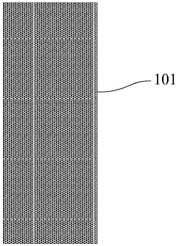
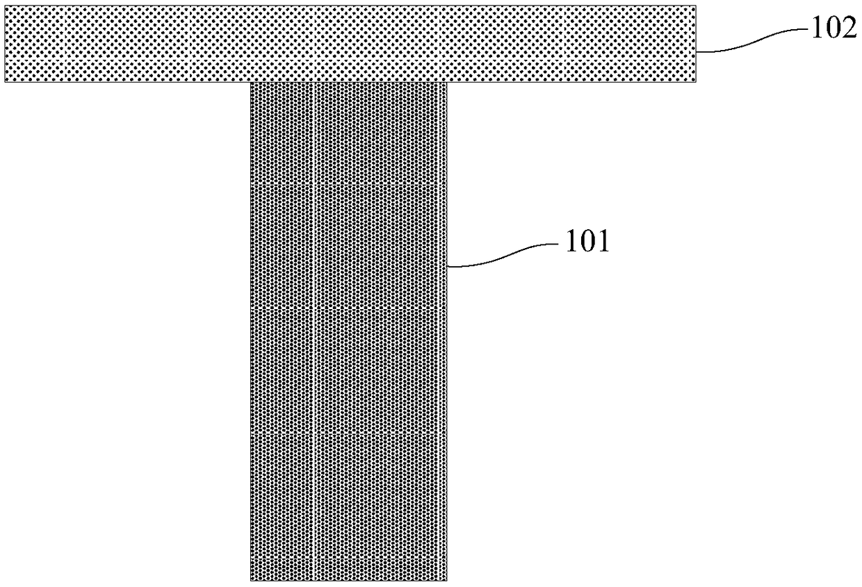
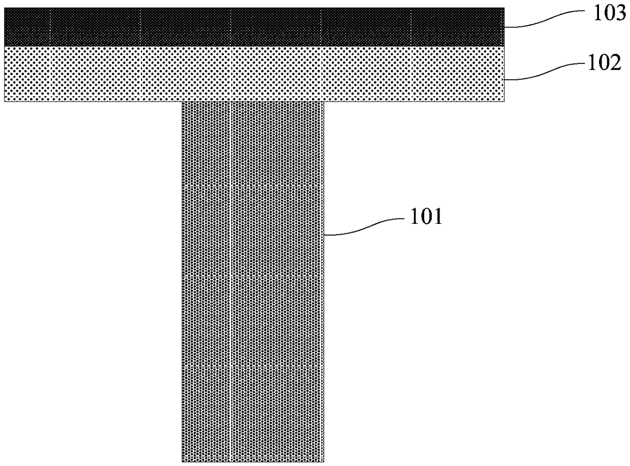
[0041] Such as Image 6 As shown, this embodiment provides a schematic structural diagram of a 1S1R phase-change memory cell, and the 1S1R phase-change memory cell includes a lower electrode layer 101, an intermediate electrode layer 103, an upper electrode layer 105, and an electrode layer located between the lower electrode layer 101 and the The threshold transition material layer 102 between the middle electrode layer 103 and the phase change memory material layer 104 between the middle electrode layer 103 and the upper electrode layer 105; the threshold transition material layer 102 and the phase change memory material layer 104 adopts Ge-Se-Sb composite material, the chemical formula of the Ge-Se-Sb composite material is Ge x Se y Sb 100-x-y , where x and y both refer to the atomic percentage of the element, and satisfy 20<x<60, 20<y<100-x, wherein, in the threshold transition material layer 102, the atomic percentage of the Sb element satisfies 0<100-x-y <20, in the p...

Embodiment 3

[0061] This embodiment tests the electrical performance of the 1S1R phase-change memory cell in the above-mentioned embodiment 2:

[0062] The relationship between the device cell resistance and the applied pulse voltage was tested. For test results see Figure 7 . For the measured 1S1R (1S: Ge 47 Se 47 Sb 6 , 1R:Ge 32 Se 32 Sb 36 ) phase-change memory unit, under the action of a pulse with a width of 100ns, when the pulse height reaches 1.7V, the sheet resistance changes from ≈10 5 The high-impedance state of Ω / □ suddenly drops to ≈10 2 Ω / □ low resistance state; when the pulse height reaches 3.3V, the sheet resistance rises rapidly to ≈10 5 The high-impedance state of Ω / □, where Ω / □ represents the sheet resistance. The difference between the high and low resistance values ​​is about three orders of magnitude, and the stored binary values ​​can be easily distinguished when used in a memory device.


PUM

PropertyMeasurementUnit
Thicknessaaaaaaaaaa
Thicknessaaaaaaaaaa
Diameteraaaaaaaaaa

Abstract

The invention provides a Ge-Se-Sb composite material, a 1S1R phase change memory unit and a preparation method thereof. The composite material has the chemical formula of GexSeySb100-x-y, wherein x and y are both atomic percentage of elements, and a formula which is as shown in the specification is met. When the material is used as a gate device material dielectric, the atomic percentage of Sb element satisfies a formula which is as shown in the specification, and the threshold value conversion unit has the advantages of low threshold voltage, high switching ratio and the like; when the material is used as an energy storage material dielectric, the atomic percentage of Sb element satisfies a formula which is as shown in the specification, and the material is high in crystallization temperature and the phase change storage unit has relatively high data retention. The Ge-Se-Sb composite material has the threshold value transformation (OTS) characteristic as well as phase change storage (OMS) characteristic, and has the reversible conversion capability between high resistance and low resistance under the effect of an electric signal.

Description

technical field [0001] The invention belongs to the technical field of micro-nano electronics, and in particular relates to a Ge-Se-Sb composite material, a 1S1R phase-change memory unit and a preparation method. Background technique [0002] As a semiconductor device, memory has always occupied an important position in the semiconductor market. Phase change memory using phase change thin film material as storage medium is considered to be the most potential next-generation non-volatile memory. Phase-change memory technology is based on the Ovshinsky electronic effect memory proposed by S.R.Ovshinsky in the late 1960s and early 1970s. Its key materials include phase-change films as storage media, heating electrode materials, insulating materials and lead-out electrodes. materials etc. The basic principle of phase change memory is: apply electrical pulse signal to the device unit, make the phase change material produce reversible transition between the amorphous state and t...

Claims


Application Information

Patent Timeline
IPC IPC(8): H01L45/00
CPCH10N70/8825H10N70/011
Inventor 刘广宇吴良才李涛章思帆宋志棠
Owner SHANGHAI INST OF MICROSYSTEM & INFORMATION TECH CHINESE ACAD OF SCI
Why Eureka
Try Eureka