TSC ceramic film, and preparation method and application thereof

A ceramic thin film and film-forming technology, which is applied in ion implantation plating, metal material coating technology, coating, etc., can solve the problems of research in the field of optoelectronics, poor conductivity and transmittance, and infrared transmittance. Low-level problems, achieving good engineering application prospects, excellent near-infrared transmittance and conductivity, and reliable cost effects

Active Publication Date: 2018-12-04
UNIV OF ELECTRONICS SCI & TECH OF CHINA
View PDF4 Cites 3 Cited by
  • Summary
  • Abstract
  • Description
  • Claims
  • Application Information

AI Technical Summary

Problems solved by technology

[0002] In the 1960s, Nowotny and others first proposed the concept of ternary layered carbide / nitride ceramics. Since then, researchers have discovered some compounds with similar structures, but these compounds did not attract enough attention at that time.
The transmittance of ITO film to visible light can reach more than 95%, and the absorbance rate to ultraviolet rays can reach more than 85%, but the transmittance to infrared rays is very low, the highest is only about 20%.
Moreover, the ITO material itself has certain defects. For example, indium (In) is classified as a rare earth metal and is a precious metal; ITO has strong water absorption, and it is easy to absorb moisture and carbon dioxide in the air and cause chemical reactions to deteriorate, commonly known as "Moldy", so special attention should be paid to moisture-proof during storage, and a waterproof layer is usually required in actual use; the ITO layer is prone to ion replacement reactions in active positive ion solutions, forming other reactions with poor conductivity and transmittance Substances, cannot be placed in the active positive ion solution for a long time during processing
[0005] Ti 3 SiC 2 The research direction of ceramics is limited to the preparation method and its tribology research, and there is no research on it in the field of optoelectronics

Method used


Image

  • TSC ceramic film, and preparation method and application thereof
  • TSC ceramic film, and preparation method and application thereof
  • TSC ceramic film, and preparation method and application thereof

Examples


Embodiment

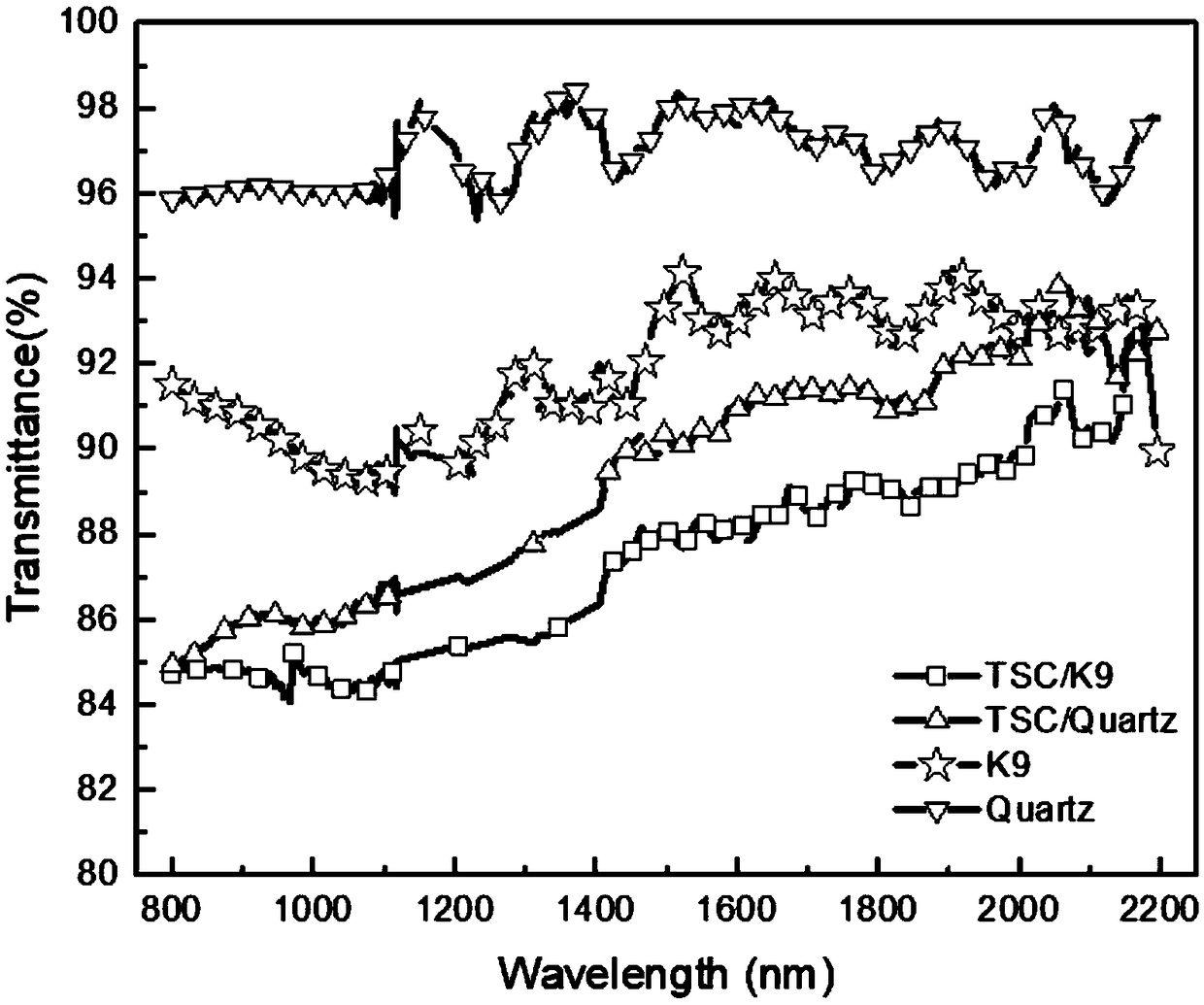
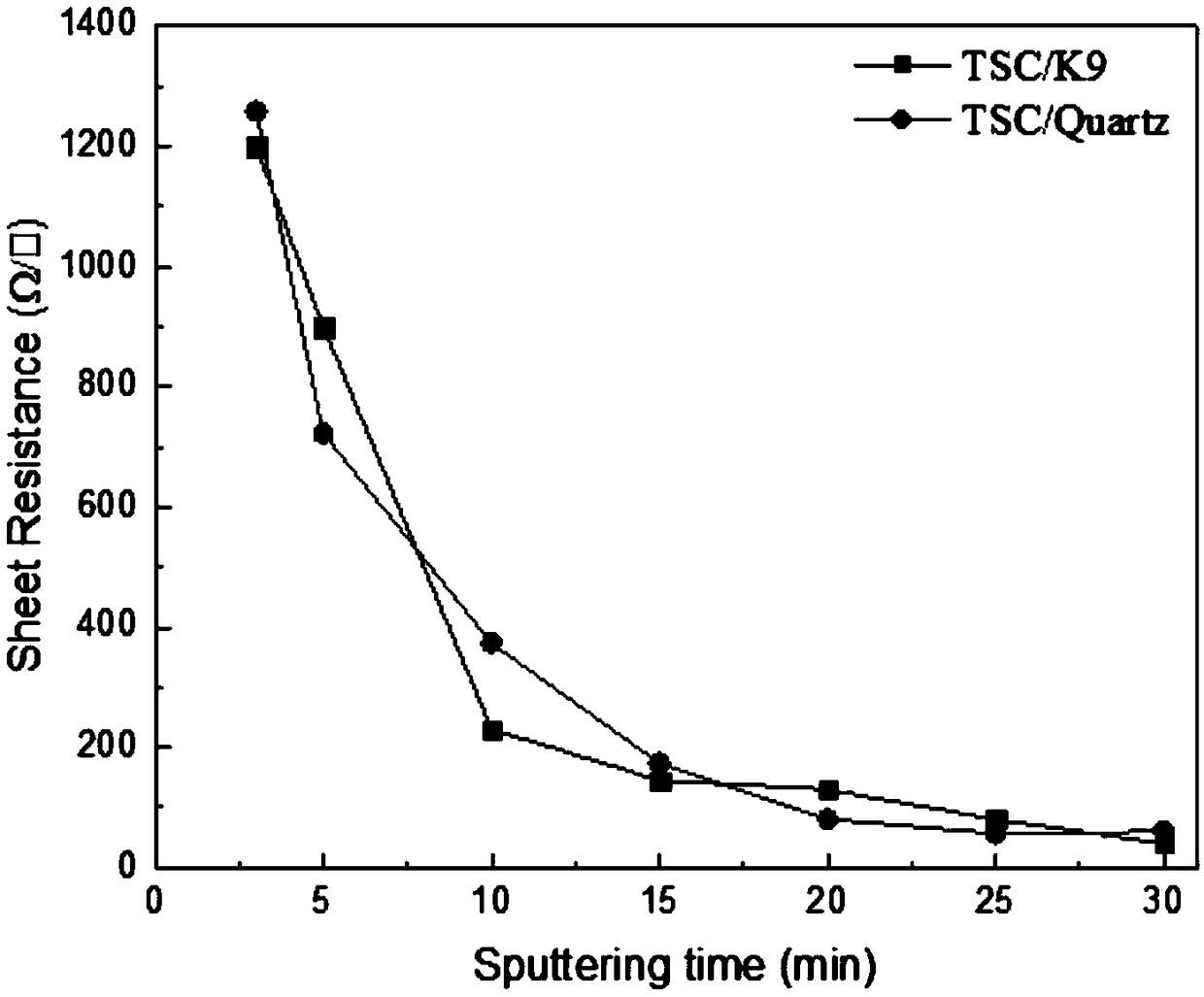
[0023] The present invention should adopt any suitable transparent substrate such as glass or quartz as the substrate, and the present embodiment adopts the K9 substrate and the quartz substrate as the substrate, adopts argon as the working gas, and conducts the process on it based on the DC sputtering method respectively. Thin film plating, prepare a kind of TSC ceramic film with high near-infrared light transmittance and conductivity, the specific operation is as follows:

[0024] Step 1: Target preparation:

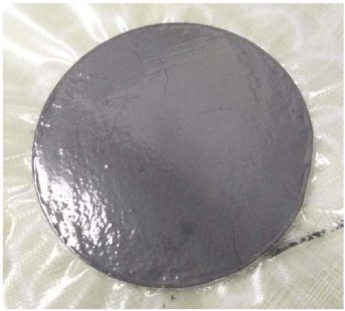
[0025] Ti 3 SiC 2 Add the powder into deionized water and stir evenly to obtain Ti 3 SiC 2 dispersion, and then the Ti 3 SiC 2 Put the dispersion into an aluminum tray with a diameter of 90mm and a thickness of 3-4mm, and then put the aluminum tray in a vacuum oven at 120°C for 24 hours and take it out. Based on the above operations, a DC sputtering target is prepared. It should be vacuum-sealed and placed. For the target, please refer to the attached figure 1 ; ...


PUM

PropertyMeasurementUnit
thicknessaaaaaaaaaa
melting pointaaaaaaaaaa
diameteraaaaaaaaaa

Abstract

The invention discloses a TSC ceramic film, and a preparation method and an application thereof, and belongs to the technical field of photoelectric materials. The semiconductor film with a micro-nanothickness is prepared in traditional physical vapor deposition (PVD) coating manner by using a Ti3SiC2 powder material as a target material. The preparation method has the advantages of simplicity, reliability and low cost, and the prepared film keeps the good mechanical performances and friction wearing performance of the Ti3SiC2 material, and also has dual performances of near-infrared lights and moderate conductivity. The Ti3SiC2 ceramic film obtained by the method has a transmittance of 80% or above and a conductivity of 50- 2000 omega/square in a spectral range of 800-2200 nm, so the application range of the Ti3SiC2 material can be broadened to the technical field of photoelectricity based on the above properties, and the Ti3SiC2 material provides a theoretical basis for packaging ofinfrared band photoelectric devices as a window material. The ceramic film of the invention has good engineering application prospects in the field of photoelectricity.

Description

technical field [0001] The invention belongs to the technical field of photoelectric materials, and in particular relates to a preparation method of a TSC ceramic thin film and its product and application. Background technique [0002] In the 1960s, Nowotny and others first proposed the concept of ternary layered carbide / nitride ceramics. Since then, researchers have discovered some compounds with similar structures, but these compounds did not attract enough attention at that time. In 2000, Barsoum published an article on "M n+1 AX n phase" (referred to as MAX phase) materials, and the review also introduces a series of advantages of this type of ceramic materials, which have both ceramic and metal properties. Like ceramics, they have a high melting point, High temperature strength and yield strength, good oxidation resistance, corrosion resistance and thermal shock resistance; like metals, they have high thermal and electrical conductivity, high shear modulus and elastic...

Claims


Application Information

Patent Timeline
Patent Type & Authority Applications(China)
IPC IPC(8): C23C14/34C23C14/06
CPCC23C14/0635C23C14/34
Inventor 次会聚宋宇浩陈奕丞赵昕祁康成李伟
Owner UNIV OF ELECTRONICS SCI & TECH OF CHINA
Why Eureka
Try Eureka