Method for preparing single-layer multilayer graphene thermoelectric detector through laser ablation

A multi-layer graphene, pyroelectric detector technology, applied in the manufacture/processing of thermoelectric devices, final product manufacturing, sustainable manufacturing/processing, etc., can solve the problems of complex preparation process, achieve simple overall structure and fast response speed , easy to achieve effect

Active Publication Date: 2018-12-07
SHANGHAI UNIVERSITY OF ELECTRIC POWER
View PDF12 Cites 5 Cited by
  • Summary
  • Abstract
  • Description
  • Claims
  • Application Information

AI Technical Summary

Problems solved by technology

[0005] Chinese patent CN104979464B discloses a flexible thermoelectric conversion device based on graphene heterojunction, including a flexible substrate layer, a dielectric layer grown sequentially on the flexible substrate layer, a first graphene layer, a second graphene layer, a first graphite The ene layer and the second graphene layer are overlapped to form a heterojunction. The first metal electrode is grown on the first graphene layer, and the second metal electrode is grown on the second graphene layer. The patent obtains graphite through a standard mechanical exfoliation process. Graphene, and find a single layer of graphene through an optical microscope, and measure the Raman scattering spectrum through a microscope to determine the actual number of layers of the selected graphene, and then transfer it to the dielectric layer by transfer technology, the preparation process is more complicated

Method used


Image

  • Method for preparing single-layer multilayer graphene thermoelectric detector through laser ablation
  • Method for preparing single-layer multilayer graphene thermoelectric detector through laser ablation
  • Method for preparing single-layer multilayer graphene thermoelectric detector through laser ablation

Examples


Embodiment 1

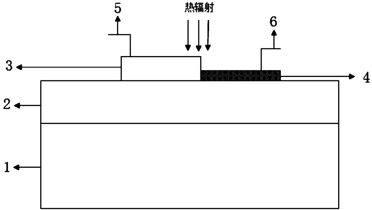
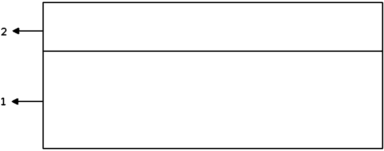
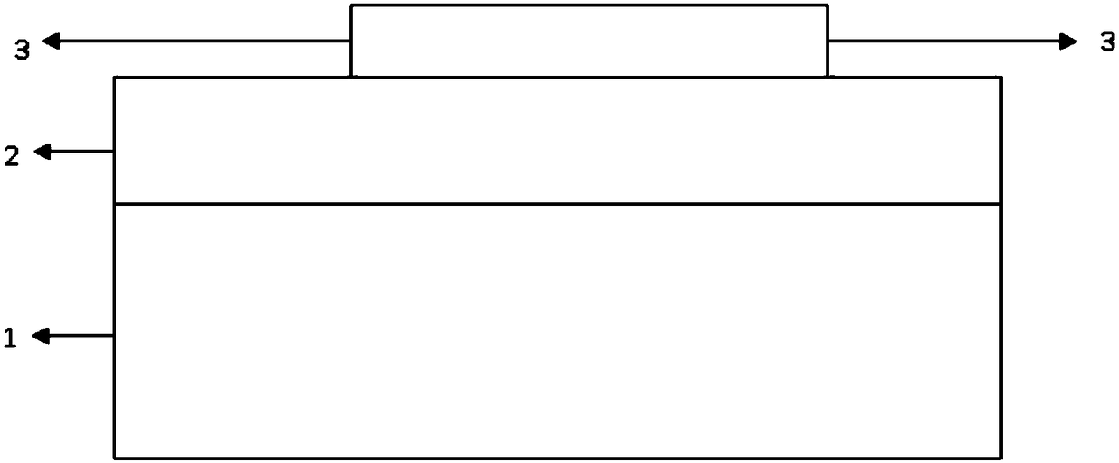
[0031] Such as figure 1 As shown, the graphene monolayer multilayer pyroelectric detector prepared by laser ablation, refer to Figure 2-4 The preparation steps of the thermoelectric device are as follows: growing a layer of insulating dielectric layer 2 on the substrate material 1, transferring a layer of multilayer graphene layer 3 on the insulating dielectric layer 2, and performing laser direct writing on the multilayer graphene layer 3 The ablated multi-layer graphene layer 3 becomes a single-layer graphene layer 4.

[0032] Deposit the first metal electrode 5 at one end of the multilayer graphene layer 3 without ablation, and deposit the second metal at one end of the thin film from the multilayer graphene layer 3 to the single layer graphene layer 4 after laser ablation Electrode 6. Based on the characteristics of multi-layer graphene film thinned into single-layer graphene film after laser ablation, a multi-layer-single-layer graphite heterostructure is generated ins...

Embodiment 2

[0036] In this embodiment, the material of the substrate is flexible polyethylene naphthalate, the dielectric layer is a silicon nitride dielectric layer, and the thickness of the silicon nitride dielectric layer is 100 nm; the thickness of the multilayer graphene 3 is 20 nm.

[0037] During the preparation, the multilayer graphene was obtained by standard mechanical exfoliation process, and then transferred to the silicon nitride dielectric layer, and then the multilayer graphene layer was ablated with a laser energy of 20 mW. Finally, the electron beam evaporation method was used to separate A metal diaphragm is deposited on one end of the multi-layer graphene and one end of the single-layer graphene, and then a first metal electrode and a second metal electrode are manufactured through a lift-off process. In this embodiment, the first metal electrode and the second metal electrode both have a thickness of 100 nm and are made of aluminum. All the other are with embodiment 1....

Embodiment 3

[0039] In this embodiment, the material of the substrate is polyimide, the dielectric layer is an alumina dielectric layer, and the thickness of the alumina dielectric layer is 200nm; a multi-layer two-dimensional material layer is transferred on the dielectric layer, and the two-dimensional material The layer is a multilayer molybdenum disulfide thin film, and the thickness of the molybdenum disulfide layer is 16 nm.

[0040] During preparation, a multilayer molybdenum disulfide thin film is prepared by a high-temperature vacuum synthesis method, and then transferred to an alumina dielectric layer, and then a laser is used to irradiate the multilayer molybdenum disulfide thin film, and the laser energy is 10 milliwatts. Finally, a metal diaphragm is deposited on one end of the non-ablated multi-layer molybdenum disulfide film 3 and the ablated single-layer molybdenum disulfide film by thermal evaporation, and then the first metal diaphragm is made through a lift-off process. ...


PUM

PropertyMeasurementUnit
thicknessaaaaaaaaaa
thicknessaaaaaaaaaa
thicknessaaaaaaaaaa

Abstract

The invention relates to a method for preparing a single-layer multilayer graphene thermoelectric detector through laser ablation. The method comprises the following steps that an insulating dielectric layer is grown on substrate material; a layer of multilayer graphene film is transferred from the insulating dielectric layer; laser ablation is performed on a part of multilayer graphene films so that a part of multilayer graphene films become a single layer of graphene film; and a first metal electrode is deposited on one end of the multilayer graphene films without ablation and a second metalelectrode is deposited on one end of the single layer of graphene film obtained through laser ablation so that the single-layer multilayer graphene thermoelectric detector can be obtained. The multilayer graphene and the single-layer graphene have the seebeck coefficient difference, and the thermal voltage is generated because of temperature difference at the heterojunction interface due to the interlayer thermal conductivity difference between the substrate and the graphene in case of light irradiation so that the thermal current can be detected at the first and second metal electrodes. Theconstructed thermoelectric detector has the advantages of simple manufacturing method, small volume and high detection sensitivity.

Description

technical field [0001] The invention relates to the technical field of graphene pyroelectric detectors, in particular to a method for preparing monolayer and multilayer graphene pyroelectric detectors by laser ablation. Background technique [0002] Graphene materials have a unique zero-gap energy band structure and electrical properties of near-ballistic transport. Compared with traditional semiconductor detectors, the detectors constructed by it have a wider detection spectrum range, faster response speed and higher cut-off frequency. Multilayer graphene and single-layer graphene have different energy band structures and densities of states. When laser ablation is performed, the interlayer thermal conductivity of multilayer graphene is poor, and heat accumulates between layers, and multilayer graphene will be destroyed. Oxidation, thickness reduction, and graphene layer number reduction; when the thickness of graphene is reduced to a single layer, because of its good therm...

Claims


Application Information

Patent Timeline
Patent Type & Authority Applications(China)
IPC IPC(8): H01L35/34
CPCH10N10/01Y02P70/50
Inventor 汤乃云
Owner SHANGHAI UNIVERSITY OF ELECTRIC POWER
Why Eureka
Try Eureka