Transparent conducting layer for heterojunction solar cell and heterojunction solar cell

A transparent conductive layer, solar cell technology, applied in circuits, photovoltaic power generation, electrical components, etc., can solve the problems of expensive reactive sputtering deposition equipment, expensive indium elements, and high production costs, and achieve transmission and collection. Chemical effect, good mechanical properties

Inactive Publication Date: 2018-12-18
SHANGHAI ADVANCED RES INST CHINESE ACADEMY OF SCI +1
View PDF7 Cites 0 Cited by
  • Summary
  • Abstract
  • Description
  • Claims
  • Application Information

AI Technical Summary

Problems solved by technology

[0004] In view of the shortcomings of the prior art described above, the object of the present invention is to provide a transparent conductive layer for heterojunction solar cells and a heterojunction solar cell to solve the problems in the prior art heterojunction solar cells. The use of indium element in the transparent conductive layer has the problems of high price of indium element, expensive reactive sputtering deposition equipment, high process temperature and high production cost

Method used


Image

  • Transparent conducting layer for heterojunction solar cell and heterojunction solar cell
  • Transparent conducting layer for heterojunction solar cell and heterojunction solar cell
  • Transparent conducting layer for heterojunction solar cell and heterojunction solar cell

Examples


Embodiment 1

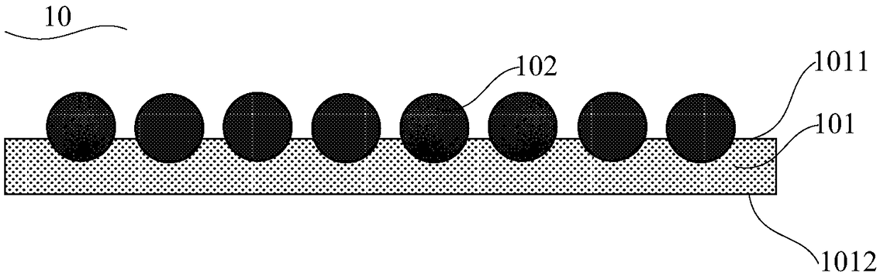
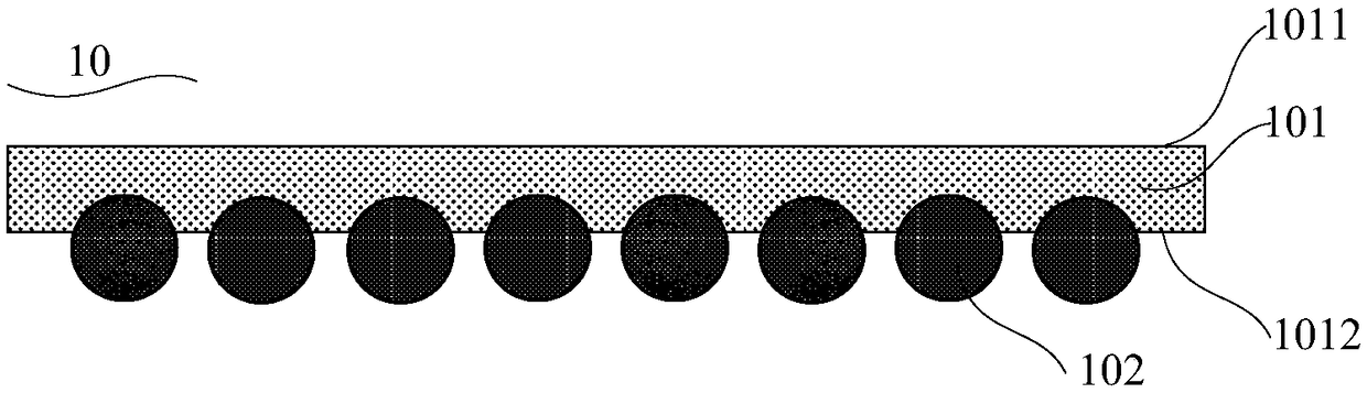
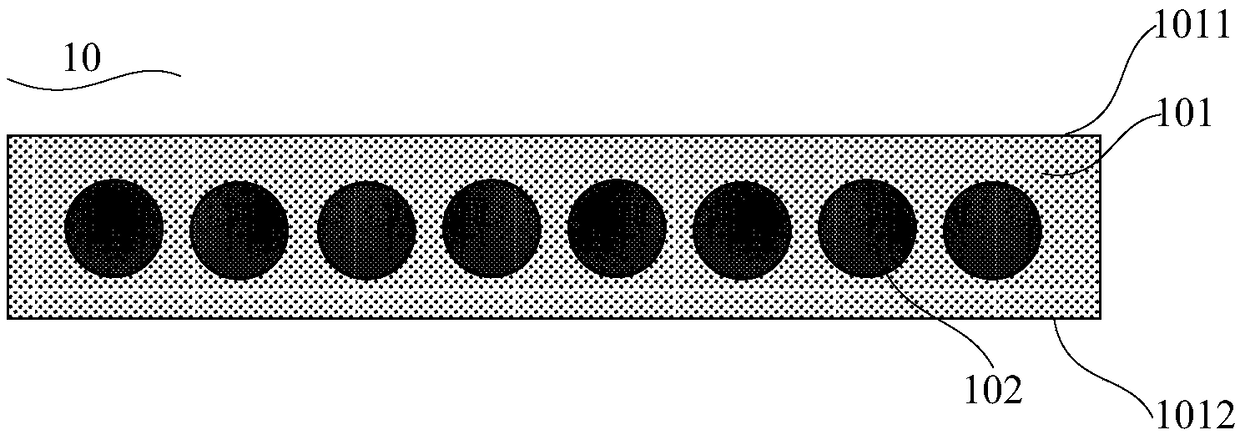
[0067] see Figure 1 to Figure 3 , this embodiment provides a transparent conductive layer 10 for a heterojunction solar cell, the transparent conductive layer 10 comprising:

[0068] Conductive polymer layer 101, described conductive polymer layer 101 comprises opposite first surface 1011 and second surface 1012;

[0069] A one-dimensional conductive material 102 , the one-dimensional conductive material 102 is located on at least one of two opposite surfaces of the conductive polymer layer 101 , or is covered inside the conductive polymer layer 101 .

[0070] In one example, the conductive polymer layer 101 can be at least any one of dipping, spin coating, blade coating, spray coating, wet coating, screen printing, roller coating and plate coating at room temperature. After coating, it is formed by drying and curing at 120-180°C. The one-dimensional conductive material 102 is formed by dipping and pulling, spin coating, blade coating, spray coating, wet coating, screen prin...

Embodiment 2

[0087] Please combine Figure 4 , the present invention also provides a heterojunction solar cell, the heterojunction solar cell comprising:

[0088] A silicon-based substrate 11, said silicon-based substrate 11 comprising a first surface and a second surface opposite to each other;

[0089] A first intrinsic silicon-based thin film layer 12, the first intrinsic silicon-based thin film layer 12 is located on the first surface of the silicon-based substrate 11;

[0090] A second intrinsic silicon-based thin film layer 13, the second intrinsic silicon-based thin film layer 13 is located on the second surface of the silicon-based substrate 11;

[0091] A first doped silicon-based thin film layer 14, the first doped silicon-based thin film layer 14 is located on the surface of the first intrinsic silicon-based thin film layer 12 away from the silicon-based substrate 11;

[0092] The second doped silicon-based thin film layer 15, the second doped silicon-based thin film layer 15 ...

Embodiment 3

[0100] see Figure 5 , the present invention also provides a heterojunction solar cell. The specific structure of the heterojunction solar cell described in this embodiment is roughly the same as the specific structure of the heterojunction solar cell described in Embodiment 2. The difference is: the second transparent conductive layer in the heterojunction solar cell described in Embodiment 2 is the transparent conductive layer 10 described in any one of Embodiment 1, while the heterojunction solar cell described in this embodiment The second transparent conductive layer in the solar cell is an indium oxide-based transparent oxide conductive thin film layer 16 (indium oxide-based TCO thin film).

[0101] Other structures of the heterojunction solar cell described in this embodiment are the same as those corresponding to the heterojunction solar cell described in Embodiment 2, please refer to Embodiment 2 for details, and will not be repeated here.


PUM


Abstract

The present invention provides a transparent conducting layer for a heterojunction solar cell and a heterojunction solar cell. The transparent conducting layer comprises a conducting polymer layer including an opposite first surface and second surface. A one-dimensional conducting material located on at least one surface of the opposing surfaces of the conducting polymer layer or coated inside theconducting polymer layer. The invention reduces or even avoids the use of rare indium element with high valence, and can remarkably reduce the production cost; The process is simple, does not need high-priced vacuum equipment, does not need high-temperature process, more suitable for heterojunction batteries; At the same time, the light transmittance of the transparent conducting layer of the invention is equivalent to that of the existing indium oxide-based thin film, and the transparent conducting layer has high conductivity, so that the consumption of the metal electrode paste can be reduced; Compared with the existing indium oxide-based thin films, the cost is lower and the mechanical properties are better, which can be widely used in flexible devices.

Description

technical field [0001] The invention relates to the technical field of solar cell photovoltaics, in particular to a transparent conductive layer for a heterojunction solar cell and the heterojunction solar cell. Background technique [0002] HIT (Heterojunction with Intrinsic Thin-Layer) cell is a high-efficiency heterojunction silicon-based solar cell, a heterogeneous crystalline silicon solar cell with an ultra-thin intrinsic hydrogenated amorphous silicon layer, which has the advantages of high conversion efficiency and low production cost. In recent years, through the continuous exploration of new materials and the continuous optimization of the device manufacturing process, the conversion efficiency and production cost of HIT cells have been further reduced, and the transition from the laboratory to large-scale commercial applications has been realized. The traditional HIT battery is prepared on the n-type single crystal Si wafer after surface texture, from the front su...

Claims


Application Information

Patent Timeline
IPC IPC(8): H01L31/0224H01L31/074
CPCH01L31/022466H01L31/074Y02E10/50
Inventor 方小红姜祥玉王继磊李高非杨立友陈小源鲁林峰李东栋
Owner SHANGHAI ADVANCED RES INST CHINESE ACADEMY OF SCI
Why Eureka
Try Eureka