

An organic photodetector for a wide spectrum and a preparation method thereof
A photodetector and wide-spectrum technology, which is applied in photovoltaic power generation, electric solid-state devices, semiconductor/solid-state device manufacturing, etc., can solve problems such as complex processes, achieve simple processes, expand the spectral response range, and improve the effect of photogenerated current
- Summary
- Abstract
- Description
- Claims
- Application Information
AI Technical Summary
Problems solved by technology
Method used
Image

Examples
preparation example Construction
[0049] A kind of preparation method of the organic photodetector that is used for broad spectrum of the present invention, specifically comprises the following steps:
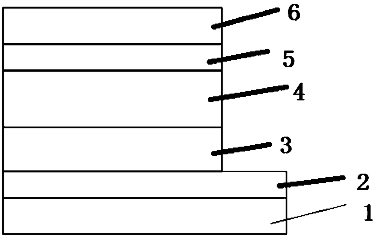
[0050] Step 1, first coat the ITO electrode layer 2 on the glass substrate 1, then use a wet method to clean the glass substrate 1 coated with the ITO electrode layer, and then dry it with pure nitrogen or infrared;
[0051] The process of wet cleaning is as follows: firstly use deionized water to ultrasonically clean the glass substrate 1 for 15 minutes to 20 minutes, then use acetone to ultrasonically clean the glass substrate 2 for 15 minutes to 20 minutes, and finally use absolute ethanol to ultrasonically clean it for 15 minutes to 20 minutes.
[0052] Step 2: After cleaning the glass substrate 1 treated in step 1 with ultraviolet ozone light, it is placed in a nitrogen glove box, and the PEDOT:PSS mixture is spin-coated on the surface of the ITO electrode layer 2 by a glue homogenizer, and spin-coated The...
Embodiment 1
[0059] Step 1, first coat the ITO electrode layer 2 on the glass substrate 1, then use a wet method to clean the glass substrate 1 coated with the ITO electrode layer, and then dry it with pure nitrogen or infrared;
[0060] The process of wet cleaning is as follows: first, the glass substrate 1 is ultrasonically cleaned with deionized water for 15 minutes, then the glass substrate 2 is ultrasonically cleaned with acetone for 15 minutes, and finally, the glass substrate 2 is ultrasonically cleaned with absolute ethanol for 15 minutes.
[0061] Step 2: After cleaning the glass substrate 1 treated in step 1 with ultraviolet ozone light, it is placed in a nitrogen glove box, and the PEDOT:PSS mixture is spin-coated on the surface of the ITO electrode layer 2 by a glue homogenizer, and spin-coated The speed is 3000rpm, and the spin-coating time is 60s; after the spin-coating is completed, place the glass substrate 1 on a sample heating table at 120°C for annealing for 15min to form...
Embodiment 2
[0067] Step 1: first coat the ITO electrode layer 2 on the glass substrate 1, then use the wet method to clean the glass substrate 1 coated with the ITO electrode layer, and then dry it with pure nitrogen or infrared;
[0068] The process of wet cleaning is as follows: first, the glass substrate 1 is ultrasonically cleaned with deionized water for 15 minutes, then the glass substrate 2 is ultrasonically cleaned with acetone for 15 minutes, and finally, the glass substrate 2 is ultrasonically cleaned with absolute ethanol for 15 minutes.
[0069] Step 2: After cleaning the glass substrate 1 treated in step 1 with ultraviolet ozone light, it is placed in a nitrogen glove box, and the PEDOT:PSS mixture is spin-coated on the surface of the ITO electrode layer 2 by a glue homogenizer, and spin-coated The speed is 3200rpm, and the spin-coating time is 60s; after the spin-coating is completed, the glass substrate 1 is annealed for 15min on a sample heating table at 120°C to form an an...
PUM
 Abstract
Description
Claims
Application Information