Magnetic-field vector sensor and manufacture technology method
A magnetic field sensor, magnetic field vector technology, applied in the size/direction of the magnetic field, the use of electromagnetic devices for magnetic field measurement, magnetic variable measurement and other directions, can solve the problems of inability to achieve space magnetic vector measurement, large cross-interference, poor sensitivity consistency, etc. Achieve the effect of improving the consistency of magnetic sensitivity, eliminating cross-interference and improving magnetic sensitivity
- Summary
- Abstract
- Description
- Claims
- Application Information
AI Technical Summary
Problems solved by technology
Method used
Image
Examples
Embodiment approach
[0092] According to a preferred embodiment of the present invention, the poly / magnetic permeable microstructure is made of high magnetic permeability materials, and the high magnetic permeability materials include elemental magnetic materials and alloy magnetic materials.
[0093] In a further preferred embodiment, the elemental magnetic material is one or more of Fe, Co or Mn, and / or
[0094] The alloy magnetic material is Mn-Zn ferrite, Sendai alloy (Fe-Si-Al), molybdenum-iron alloy (MoFe), vanadium-iron alloy (VFe), tungsten-iron alloy (WFe) or nickel-iron alloy (NiFe) one or more.
[0095] In a further preferred embodiment, the poly / magnetic permeable microstructure is made of low coercivity material, preferably nickel-iron alloy (NiFe).
[0096] Wherein, the coercive force means that after the magnetic material is saturated and magnetized, its magnetic induction intensity B does not return to zero when the external magnetic field returns to zero, and the magnetic inducti...
Embodiment 1
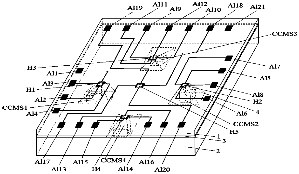
[0163] The following steps are used to make the magnetic field vector sensor:
[0164] Step 1, cleaning the first silicon wafer and the second silicon wafer (both are oriented p-type single crystal silicon wafers), and then growing a 650nm thick silicon dioxide layer on the upper surface of the second silicon wafer;
[0165] Step 2, using a bonding process to bond the first silicon wafer to the second silicon wafer, so that the lower surface of the first silicon wafer and the upper surface of the second silicon wafer are bonded as one;
[0166] Step 3, after bonding, thin the first silicon wafer to 10 μm, perform polishing and cleaning treatment, and then grow a thin oxide layer with a thickness of 50 nm on the upper surface of the first silicon wafer;
[0167] Step 4, perform a photolithography on the upper surface of the first silicon wafer, and implant ions for n - Type lightly doped to form the magnetically sensitive areas of the five Hall magnetic field sensors;
[016...
experiment example
[0178] Using Beijing Cuihai Jiacheng Magnetic Technology Co., Ltd.’s fully automatic Hall effect high-precision magnetic field generation system (CH-100) and other instruments to build a magnetic field sensor characteristic test system, the system can generate a magnetic induction intensity ranging from -0.8T to 0.8 T, the precision is 0.03mT. Using the above-mentioned high-precision magnetic field generating system, the magnetic field vector sensor prepared in Example 1 was tested, and the magnetic sensitivity detected by the sensor was analyzed.
[0179] It can be seen from the test that the magnetic field vector sensor prepared in Example 1 can successfully detect the magnetic induction intensity of -60mT~60mT in the space.
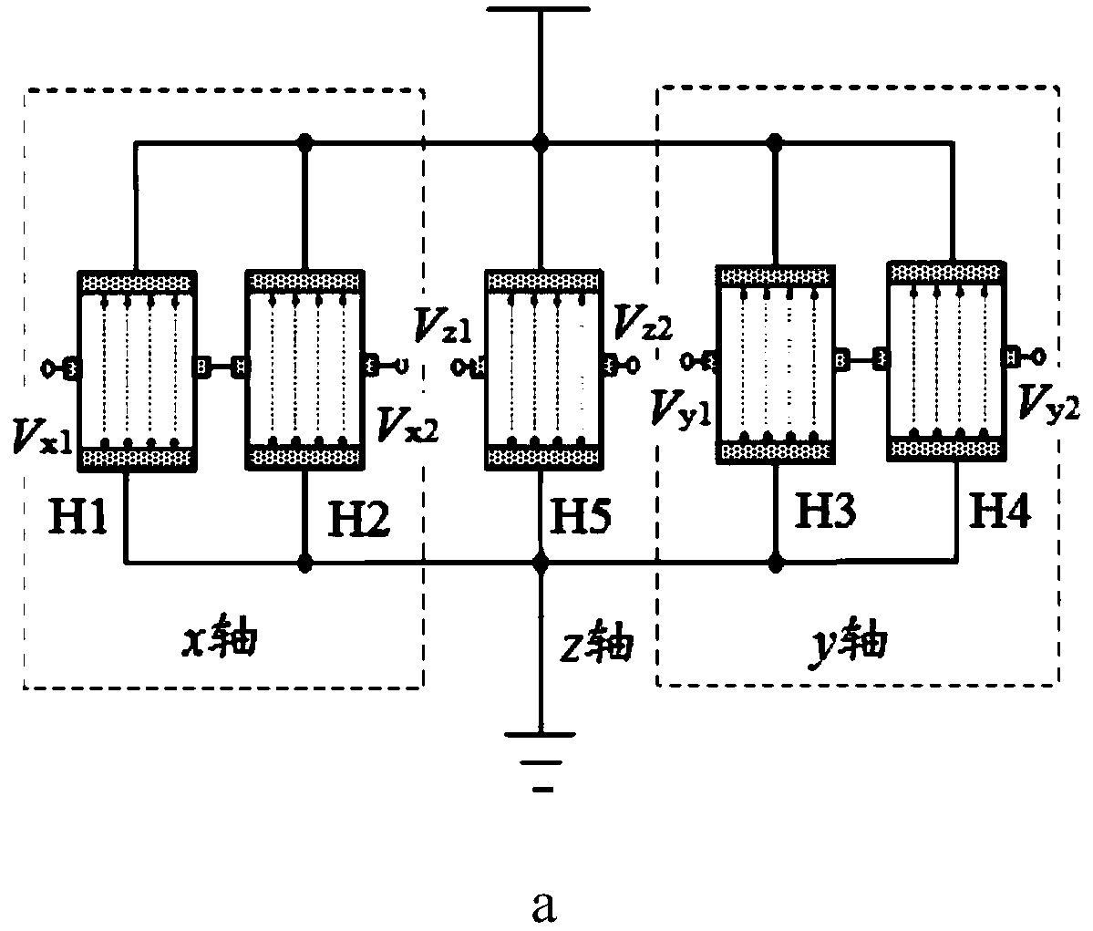
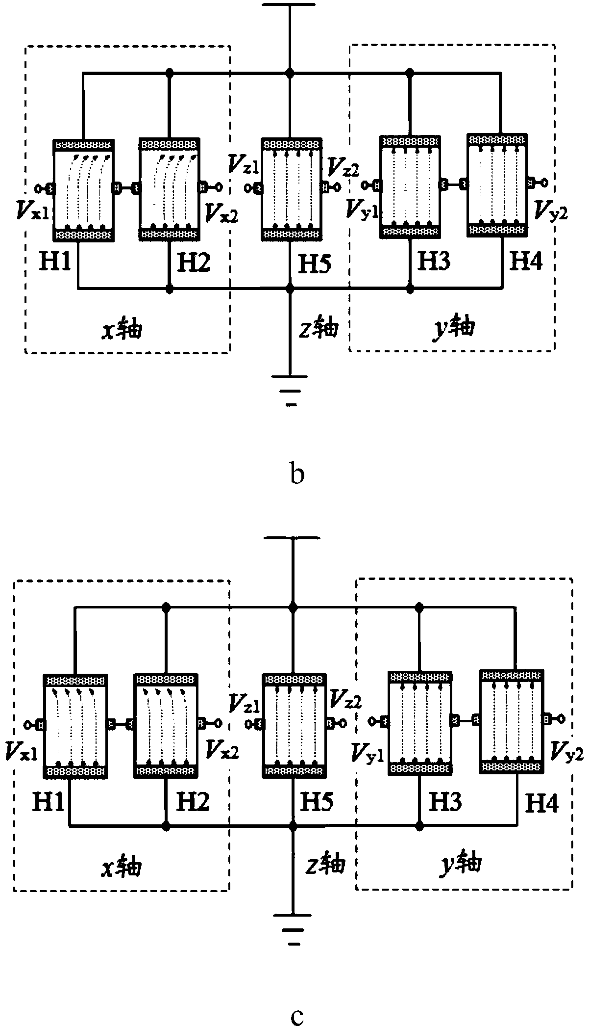
[0180] In addition, when the power supply voltage is 5V, the applied magnetic field is B=-60~60mT, the step size is 10mT, and the magnetic field direction is along the x-axis, y-axis and z-axis respectively, the input of the magnetic field vector senso...
PUM
 Abstract
Description
Claims
Application Information


