A method for preparing high-quality thick film AlN based on a nano-pattern silicon substrate

A nano-patterning and substrate technology, applied in semiconductor/solid-state device manufacturing, electrical components, circuits, etc., can solve the problems of increasing the growth cycle and increasing the cost of epitaxy, so as to improve the thickness of epitaxy, improve crystal quality and device performance, reduce Effect of defect density

Active Publication Date: 2018-12-28
北京中博芯半导体科技有限公司
View PDF8 Cites 8 Cited by
  • Summary
  • Abstract
  • Description
  • Claims
  • Application Information

AI Technical Summary

Problems solved by technology

This technology can form periodic air gaps at the interface between AlN and Si substrates by patterning the Si substrate, and use these air gaps to release the stress of the AlN film and improve the crys

Method used


Image

  • A method for preparing high-quality thick film AlN based on a nano-pattern silicon substrate
  • A method for preparing high-quality thick film AlN based on a nano-pattern silicon substrate
  • A method for preparing high-quality thick film AlN based on a nano-pattern silicon substrate

Examples


Embodiment 1

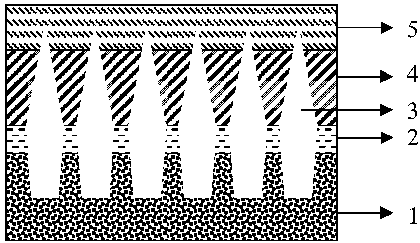
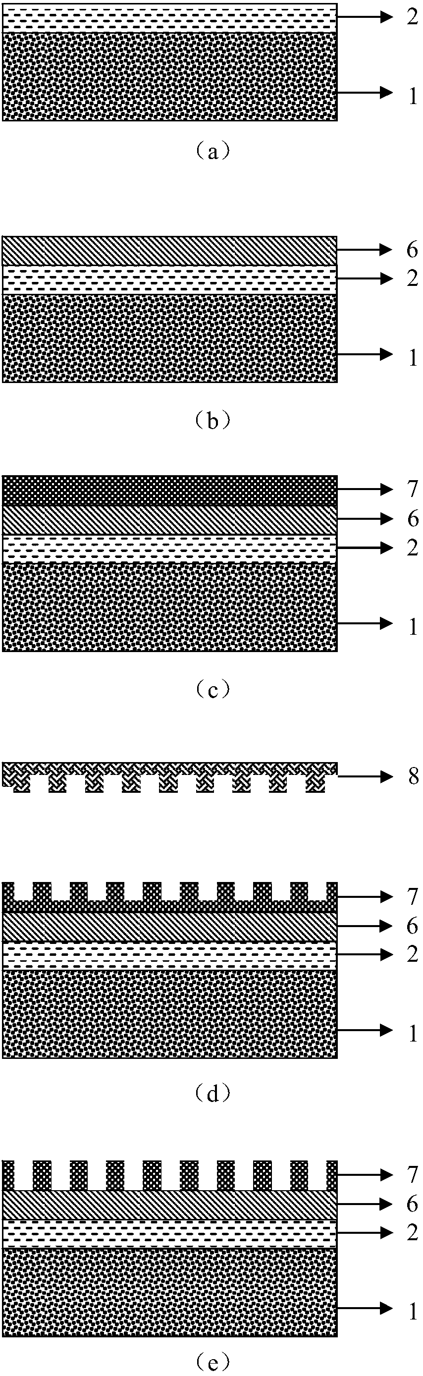
[0048] For the preparation process of high-quality thick-film AlN materials on nano-patterned Si substrates, see figure 2 , including the following steps:

[0049] (1) Select a single crystal silicon substrate 1, and the crystal orientation of silicon can be silicon (111), silicon (100), silicon (110), etc.;

[0050] (2) Growing an aluminum nitride nucleation layer 2 on a single crystal silicon substrate 1, the growth temperature is 900-1300° C., the growth pressure is 10-200 mbar, and the growth thickness is 10 nm, such as figure 2 as shown in (a);

[0051] (3) A layer of hard mask silicon dioxide 6 is deposited on the aluminum nitride nucleation layer 2 by plasma enhanced chemical vapor deposition (PECVD), the deposition temperature is 200-400 ° C, and the growth thickness is 10 nm-2 μm, like figure 2 as shown in (b);

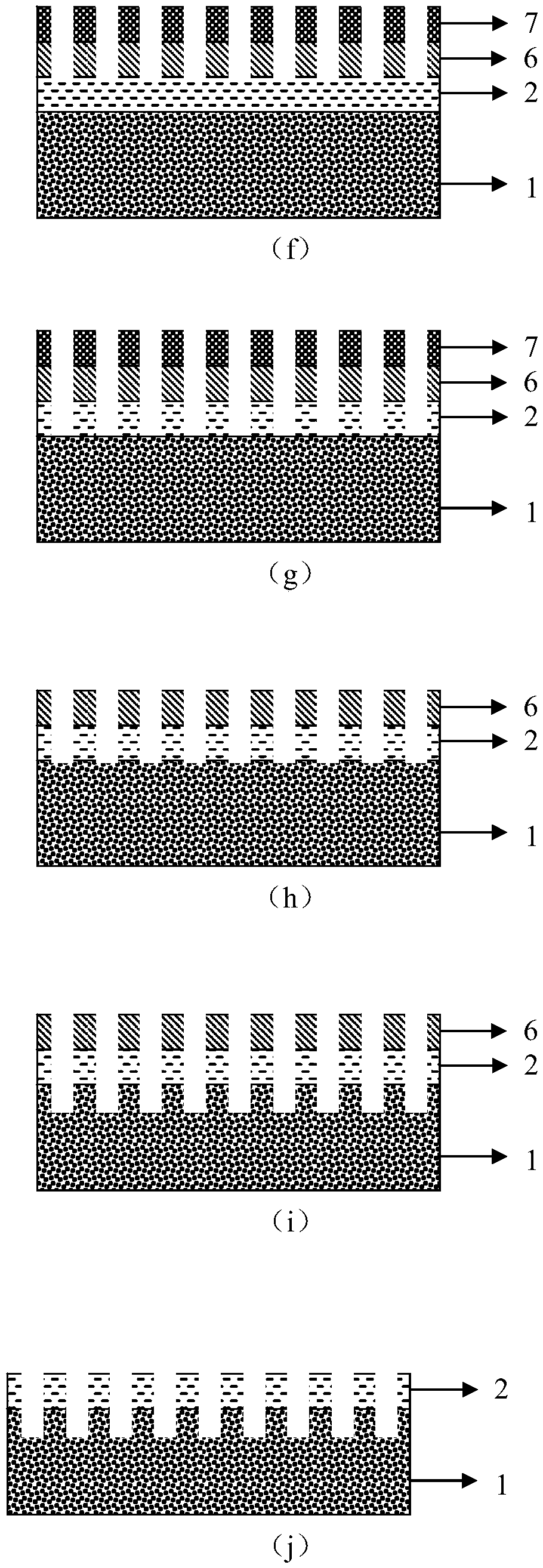
[0052] (4) Select the structure and size of the nanoimprint template, use a hexagonal hole array, the pattern period is 1 μm, the pattern aperture is 600...

Embodiment 2

[0065] Methods for preparing high-quality thick-film AlN materials on nanopatterned Si substrates see figure 2 , including the following steps:

[0066] (1) Select a single crystal silicon substrate 1, the crystal orientation of silicon can be silicon (111), silicon (100);

[0067] (2) growing the aluminum nitride nucleation layer 2 on the single crystal silicon substrate 1, the growth temperature is 900-1300°C, the growth pressure is 10-200mbar, and the growth thickness is 200nm;

[0068] (3) deposit a layer of hard mask silicon dioxide on the aluminum nitride nucleation layer 2 by plasma enhanced chemical vapor deposition (PECVD), the deposition temperature is 200-400 ° C, and the growth thickness is 10 nm-2 μm;

[0069] (4) Select the structure and size of the nanoimprint template, use a hexagonal hole array, the pattern period is 1.4 μm, the pattern aperture is 1 μm, and the pattern depth is 500 nm;

[0070] (5) spin-coating nano-imprinting adhesive with a specific thick...


PUM

PropertyMeasurementUnit
Etching depthaaaaaaaaaa
Thicknessaaaaaaaaaa
Corrosion timeaaaaaaaaaa

Abstract

The invention discloses a method for preparing high-quality thick film AlN based on a nano-pattern silicon substrate, the lamellar superimposed AlN materials obtained by the method, from the bottom up, include: a nano-patterned silicon substrate, a nano-pattern AlN nucleation layer, a high-temperature AlN transverse growth layer and a high-temperature AlN longitudinal growth layer, and a periodically arranged air gap is arranged in the nano-pattern silicon substrate, the nano-pattern AlN nucleation layer and the high-temperature AlN lateral growth layer, wherein the air gap has a depth of 10 nm to 1 mum in the Si substrate, a maximum cross-sectional width of 50 nm to 1 mum, and a period of 100 nm to 2 mum. Compared with the existing method for growing thick film AlN, the method of the invention has low cost, can be applied in large-scale industrialization, greatly reduces the defect density of AlN on the silicon substrate, improves the crystal quality of the subsequent device structurematerial, and has the advantages of low cost, low cost, low cost, and low cost, and can be used in large-scale industrialization. LED devices, MEMS, LEDs, RF filters, SAW devices and high-frequency broadband communication have broad application prospects.

Description

technical field [0001] The invention belongs to the technical field of semiconductors, and in particular relates to a substrate preparation process and an epitaxy method for obtaining high-quality thick-film AlN on a nano-patterned Si substrate. Background technique [0002] Group III nitrides as the third generation of semiconductors, including AlN, GaN and InN and their ternary and quaternary alloys, because of their excellent optical and electrical properties, especially the forbidden band width of their ternary alloys from AlN 6.1 Continuously tunable from eV to 0.64eV of InN, the corresponding band-edge emission wavelengths cover the range from 200nm in deep ultraviolet to 1.8μm in infrared. etc. have a wide range of applications. [0003] Among nitride heterostructure materials based on sapphire, silicon carbide and silicon as substrate materials, nitride-on-silicon heterostructure materials and their devices have obvious advantages in terms of large size, low cost, a...

Claims


Application Information

Patent Timeline
IPC IPC(8): H01L21/02
CPCH01L21/0254
Inventor 杨学林沈波沈剑飞张洁冯玉霞许福军王新强唐宁
Owner 北京中博芯半导体科技有限公司
Why Eureka
Try Eureka