A preparation method of a light emitting diode epitaxial wafer and a light emitting diode epitaxial wafer

A technology of light-emitting diodes and epitaxial wafers, applied in electrical components, nanotechnology, circuits, etc., can solve the problems of P-type semiconductor layers that are difficult to achieve high hole concentration and low LED luminous efficiency, so as to reduce self-compensation effect and increase III group Element vacancies, the effect of increasing concentration

Active Publication Date: 2018-12-28
HC SEMITEK ZHEJIANG CO LTD
View PDF3 Cites 6 Cited by
  • Summary
  • Abstract
  • Description
  • Claims
  • Application Information

AI Technical Summary

Problems solved by technology

[0006] The embodiment of the present invention provides a method for preparing a light-emitting diode epitaxial wafer and a light-emitting diode epitaxial wafer, which can solve the problem

Method used


Image

  • A preparation method of a light emitting diode epitaxial wafer and a light emitting diode epitaxial wafer
  • A preparation method of a light emitting diode epitaxial wafer and a light emitting diode epitaxial wafer
  • A preparation method of a light emitting diode epitaxial wafer and a light emitting diode epitaxial wafer

Examples


Embodiment Construction

[0030] In order to make the object, technical solution and advantages of the present invention clearer, the implementation manner of the present invention will be further described in detail below in conjunction with the accompanying drawings.

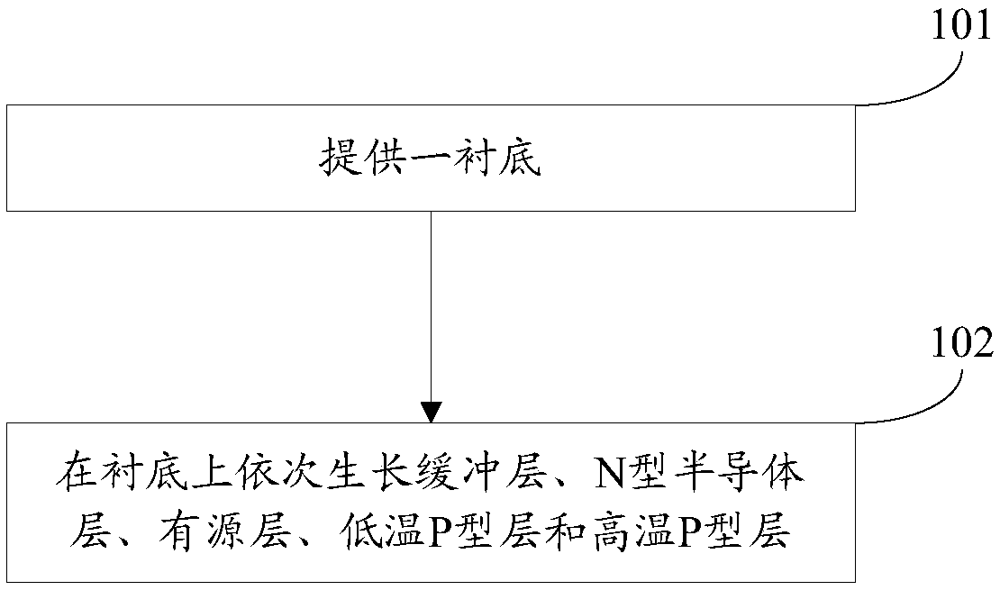
[0031] The embodiment of the present invention provides a method for preparing a light-emitting diode epitaxial wafer, figure 1 For a flowchart of a method for preparing a light-emitting diode epitaxial wafer provided by an embodiment of the present invention, see figure 1 , the preparation method comprises:

[0032] Step 101: Provide a substrate.

[0033] Specifically, the material of the substrate can be one of sapphire, silicon, and silicon carbide.

[0034] Optionally, before step 101, the preparation method may also include:

[0035] Controlling the temperature to 1000°C to 1200°C (preferably 1100°C), annealing the substrate in a hydrogen atmosphere for 1 minute to 10 minutes (preferably 8 minutes);

[0036] The substrate is n...


PUM

PropertyMeasurementUnit
Thicknessaaaaaaaaaa
Growth temperatureaaaaaaaaaa

Abstract

The invention discloses a preparation method of a light emitting diode epitaxial wafer and a light emitting diode epitaxial wafer, belonging to the field of semiconductor technology. The preparation method comprises the following steps of: providing a substrate; sequentially growing a buffer layer, an N-type semiconductor layer, an active layer, a low-temperature P-type layer and a high-temperature P-type layer on the substrate, wherein the growth temperature of the low-temperature P-type layer is lower than the growth temperature of the high-temperature P-type layer, at least one of the low-temperature P-type layer and the high-temperature P-type layer is a superlattice structure, ,the superlattice structure comprises a plurality of sub-layers stacked in sequence, and each of the sub-layers is formed by continuously passing an indium source, a gallium source, an ammonia gas and a carrier gas to form an indium gallium nitride layer; stopping the injection of the indium source and the gallium source, and simultaneously continuing to inject the ammonia gas and the carrier gas, and processing the indium gallium nitride layer; injecting a magnesium source while ammonia and a carrier gas are continuously injected to form a magnesium nitride layer on the indium gallium nitride layer. The invention can improve the concentration of holes in the superlattice structure.

Description

technical field [0001] The invention relates to the technical field of semiconductors, in particular to a method for preparing a light-emitting diode epitaxial wafer and the light-emitting diode epitaxial wafer. Background technique [0002] A light-emitting diode (English: Light Emitting Diode, referred to as: LED) is a semiconductor electronic component that can emit light. As a new type of high-efficiency, environmentally friendly and green solid-state lighting source, LED is being widely used in lighting, display screens, signal lights, backlights, toys and other fields. In the development of the light-emitting diode industry, the wide-bandgap (Eg>2.3eV) semiconductor material gallium nitride (GaN) develops very rapidly. [0003] Epitaxial wafers are the primary products in the LED manufacturing process. The existing LED epitaxial wafer includes a substrate, a buffer layer, an N-type semiconductor layer, an active layer and a P-type semiconductor layer, and the buff...

Claims


Application Information

Patent Timeline
IPC IPC(8): H01L33/00H01L33/04B82Y40/00
CPCB82Y40/00H01L33/007H01L33/04
Inventor 李昱桦乔楠刘春杨胡加辉李鹏
Owner HC SEMITEK ZHEJIANG CO LTD
Why Eureka
Try Eureka