
A method for preparing a transferable bonded PDMS-based nanostructure

A nanostructure and bonding technology, applied in the direction of nanotechnology, photoplate making process coating equipment, optomechanical equipment, etc., can solve the problems of increasing process complexity and cost, time-consuming, cumbersome steps, etc., and achieve easy cycle and occupation Empty ratio, reduce operation difficulty, and ensure the effect of flatness

Inactive Publication Date: 2019-01-01
BEIJING UNIV OF TECH
View PDF6 Cites 6 Cited by
  • Summary
  • Abstract
  • Description
  • Claims
  • Application Information

AI Technical Summary

Problems solved by technology

However, this method must adopt silanization treatment, which not only has cumbersome steps, but also increases the complexity and cost of the process, and the silanization reagent is toxic, so special attention should be paid to the experiment.
Since the separation of the PDMS film must overcome the van der Waals force, hydrogen bond and other adhesion forces between the PDMS film and the mold, and the PDMS film itself has a small thickness and low mechanical strength, it is easy to stretch, tear, and wrinkle during the separation process, resulting in damage to the microstructure
Moreover, manual operation is costly, time-consuming, and inefficient, requiring high skills, and cannot be mass-produced.
In addition, this method needs to make a mold in advance, and once the mold is prepared, the structure cannot be adjusted.
Therefore, the traditional method of preparing PDMS nanostructures has great limitations.

Method used


Image

  • A method for preparing a transferable bonded PDMS-based nanostructure
  • A method for preparing a transferable bonded PDMS-based nanostructure
  • A method for preparing a transferable bonded PDMS-based nanostructure

Examples


Embodiment Construction

[0017] The PDMS film of the nanoscale grating is prepared by using the novel method for separating the PDMS film and the rigid substrate proposed by the present invention, and the specific implementation method is as follows:

[0018] S1 configures PDMS, Sylagrd 184 silicone elastomer: the two components are mixed at a ratio of 10:1 (w / w).

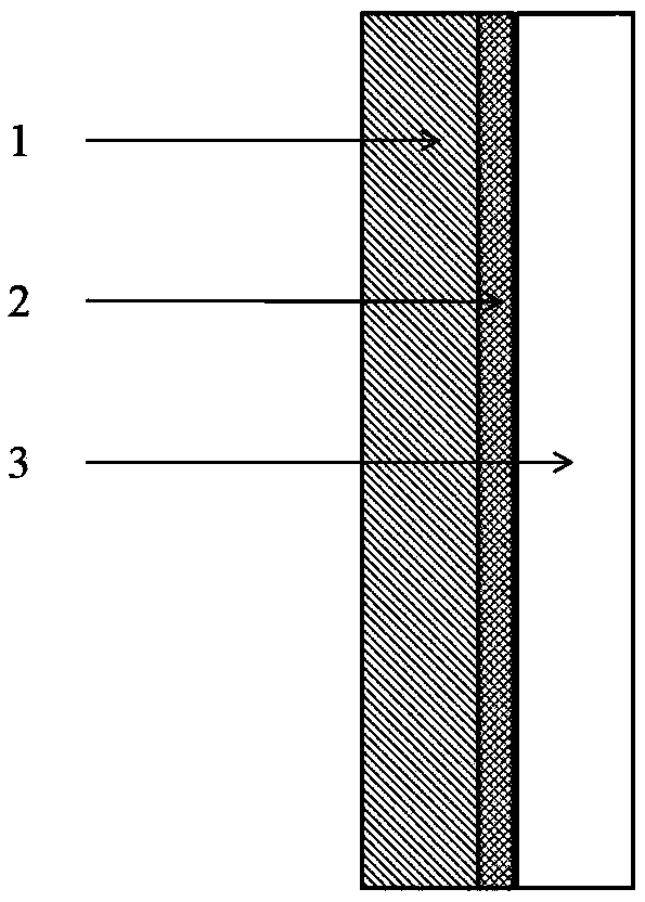
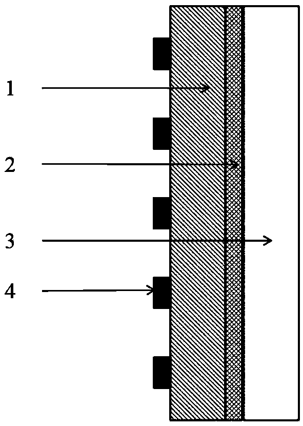
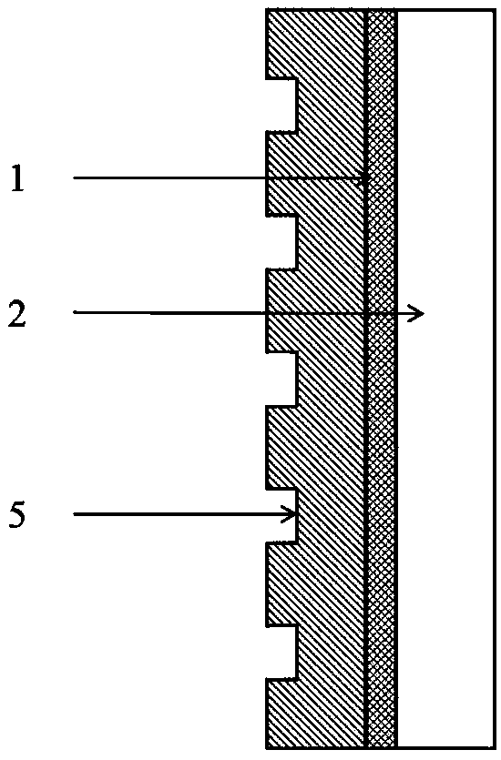
[0019] S2 Place the ITO glass substrate (3) on the glue-spinning machine, throw off a layer of photoresist (2) as a sacrificial layer, turn it forward at 1000r / min, turn it back at 1500r / min, and dry the photoresist to obtain Dried photoresist.

[0020] S3 drops the configured PDMS on the dried photoresist, and spin-coats again, the forward rotation is 1000r / min, and the back rotation is 2500r / min. The coated PDMS is left to stand for 2-3 hours to make it more smooth, and then placed on a hot plate at 100° C., and cured for 35 minutes to obtain a cured PDMS film (1).

[0021] In S4, the cured PDMS film (1) is fabricated into a nanoscale ...


PUM

PropertyMeasurementUnit
thicknessaaaaaaaaaa

Abstract

A method for preparing a transferable bonded PDMS-based nanostructure, which includes the following steps: spin coating a sacrificial layer on a rigid substrate which can be dissolved by an organic solvent such as acetone; then, spin coating a layer of PDMS on the surface of the sacrificial layer, and after curing, fabricating periodic nano-patterns on the PDMS by interference photolithography; then etching the fabricated patterns to obtain the patterned PDMS; putting the etched PDMS into an organic solvent such as acetone, dissolving the sacrificial layer, and finally obtaining the transferable bonded PDMS film with nanor-patterns. The invention uses the interference photolithography method to prepare the periodic nanometer patterns, which greatly improves the efficiency. Compared with several existing methods for preparing flexible material micro-nano structures, interference lithography has the advantages of high speed, low cost, large area, and easy period and duty cycle adjustment. The operation difficulty of film release in the fabrication process is greatly lowered, and the success rate of film fabrication is improved, and the social and economic benefits are very remarkable.

Description

technical field [0001] The invention relates to a method for manufacturing a large-area periodic nanostructure on a flexible substrate, in particular to a method for manufacturing a PDMS periodic nanostructure. Background technique [0002] PDMS (polydimethylsiloxane), namely polydimethylsiloxane, is the most widely used silicon-based organic polymer material. Solid polydimethylsiloxane is a silicone that is non-toxic, hydrophobic and water-repellent, inert, and a non-flammable, transparent elastomer. The preparation process of polydimethylsiloxane is simple and fast, and the material cost is much lower than that of silicon wafers. It has good light transmission, good biocompatibility, and is easy to bond with various materials at room temperature. It is because of the above advantages that it is widely used, including microfluidic systems, caulks, lubricants, contact lenses, etc. in biological MEMS. [0003] At present, the traditional PDMS nanostructure preparation adopt...

Claims


Application Information

Patent Timeline
Patent Type & Authority Applications(China)
IPC IPC(8): G03F7/20G03F7/16B82Y40/00
CPCB82Y40/00G03F7/16G03F7/70408
Inventor 解意洋吴俊胡良臣徐晨王秋华赵壮壮
Owner BEIJING UNIV OF TECH
Learn More