

A ternary p-type CuBi2O4 thin film transistor and a preparation method thereof
A thin-film transistor, cubi2o4 technology, applied in transistors, semiconductor/solid-state device manufacturing, electrical components, etc., can solve the problems of harsh preparation process conditions and subsequent processing processes, difficult to industrialized production and application, instability, etc., and achieve stable electrical modulation. characteristics, to achieve large-scale industrial production, the effect of simple structure
- Summary
- Abstract
- Description
- Claims
- Application Information
AI Technical Summary
Problems solved by technology
Method used
Image

Examples
Embodiment 1
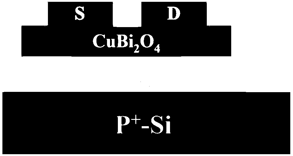
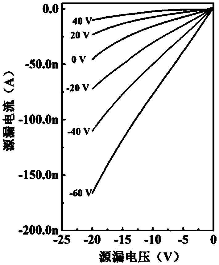
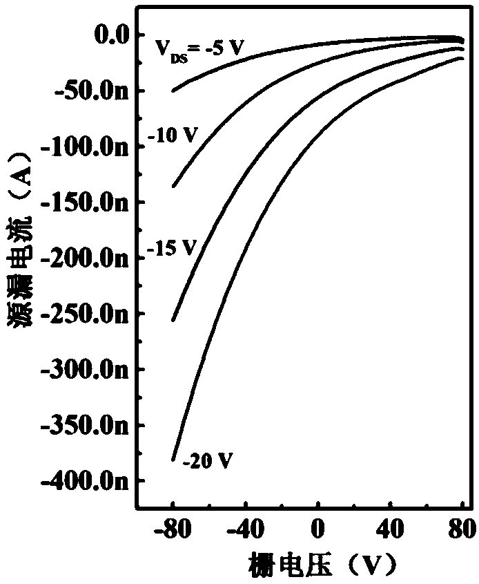
[0036] The schematic diagram of the structure of the p-type oxide thin film transistor in this embodiment is as follows figure 1 As shown, it specifically includes the following parts:
[0037] A p-type heavily doped silicon substrate is used as a gate electrode;
[0038] a silicon dioxide insulating layer grown on the above-mentioned silicon substrate by thermal oxidation;
[0039] p-type CuBi 2 o 4 a channel layer grown on the aforementioned silicon dioxide insulating layer;
[0040] Both the source and drain electrodes are gold films, which are grown on the above-mentioned channel layer.
[0041] The p-type CuBi described in this embodiment 2 o 4 A method for preparing a thin film transistor, comprising the following steps:
[0042] (1) Cleaning silicon wafers: ultrasonically clean the silicon wafers with alcohol, acetone, and deionized water for 10 minutes each to remove pollutants on the surface of the silicon wafers, and finally dry them with high-purity nitrogen ...
Embodiment 2
[0048] The schematic structural diagram of the p-type oxide thin film transistor of this embodiment is the same as that of Embodiment 1, and specifically includes the following parts:
[0049] A p-type heavily doped silicon substrate is used as a gate electrode;
[0050] a silicon dioxide insulating layer grown on the above-mentioned silicon substrate by thermal oxidation;
[0051] p-type CuBi 2 o 4 a channel layer grown on the aforementioned silicon dioxide insulating layer;
[0052] Both the source and drain electrodes are gold films, which are grown on the above-mentioned channel layer.
[0053] The p-type CuBi described in this embodiment 2 o 4 A method for preparing a thin film transistor, comprising the following steps:
[0054] (1) Cleaning silicon wafers: ultrasonically clean the silicon wafers with alcohol, acetone, and deionized water for 10 minutes each to remove pollutants on the surface of the silicon wafers, and finally dry them with high-purity nitrogen fo...
Embodiment 3
[0060] The schematic structural diagram of the p-type oxide thin film transistor of this embodiment is the same as that of Embodiment 1, and specifically includes the following parts:
[0061] A p-type heavily doped silicon substrate is used as a gate electrode;
[0062] a silicon dioxide insulating layer grown on the above-mentioned silicon substrate by thermal oxidation;
[0063] p-type CuBi 2 o 4 a channel layer grown on the aforementioned silicon dioxide insulating layer;
[0064] Both the source and drain electrodes are gold films, which are grown on the above-mentioned channel layer.
[0065] The p-type CuBi described in this embodiment 2 o 4 A method for preparing a thin film transistor, comprising the following steps:
[0066] (1) Cleaning silicon wafers: ultrasonically clean the silicon wafers with alcohol, acetone, and deionized water for 10 minutes each to remove pollutants on the surface of the silicon wafers, and finally dry them with high-purity nitrogen fo...
PUM
 Abstract
Description
Claims
Application Information