A manufacture method of high-frequency microwave board and high-density interconnect board

A technology of high-density interconnection board and manufacturing method, which is applied in chemical/electrolytic methods to remove conductive materials, printed circuit manufacturing, electrical components, etc., can solve problems such as uneven ink thickness, and achieve low defect rate and flatness Good, fine line effect

Inactive Publication Date: 2019-01-08
铜陵市超远科技有限公司
View PDF18 Cites 6 Cited by
  • Summary
  • Abstract
  • Description
  • Claims
  • Application Information

AI Technical Summary

Problems solved by technology

[0005] In order to overcome the above-mentioned technical problems, the object of the present invention is to provide a high-frequency microwave board high-density interconnection board manufacturing method, which scientifically and rationally designs cutting, drilling, plasma desmearing, copper deposition, whole board electroplating, The process of outer layer dry film, acid etching, intermediate inspection, solder mask, silk screen, forming, electrical measurement, primary product inspection, immersion tin, secondary product inspection, and packaging, compared with the existing technology, this process optimizes the drilling , Plasma treatment, solder resist, molding process methods and specific process parameter control, and precisely control the time from plasma desmear to copper deposition, acid etching to silk screen time, so that the finished product size, surface copper, hole copper, board thickness Parameters such as pore size and aperture are stable, avoiding quality defects such as no copper in the hole and uneven ink thickness, and improving the production efficiency and quality of high-frequency microwave boards and high-density interconnection boards

Method used


Image

  • A manufacture method of high-frequency microwave board and high-density interconnect board
  • A manufacture method of high-frequency microwave board and high-density interconnect board
  • A manufacture method of high-frequency microwave board and high-density interconnect board

Examples


Embodiment 1

[0039] This embodiment provides a high-density interconnection board manufacturing method for high-frequency microwave boards, including the following steps:

[0040] (1) Cutting: use a shearing machine to cut the substrate according to the size of the cut, cut the cut sheet and grind the edges. process; among them, the cutting size is 0.762mm in substrate thickness and 1 / 1OZ in copper thickness.

[0041](2) Drilling: use a new drill bit, produce according to the drilling parameters, drill the sheet metal to form a through hole, and use manual grinding on the front after drilling; specifically, the drilling parameters are: when drilling a 0.8mm hole , the feeding speed is 1.6m / min, the retracting speed is 10m / min, and the rotating speed is 60krpm; when drilling a 1.0mm hole, the feeding speed is 1.2m / min, the retracting speed is 10m / min, and the rotating speed is 50krpm; For a 1.3mm hole, the feed speed is 1.0m / min, the retract speed is 10m / min, and the rotation speed is 40kr...

Embodiment 2

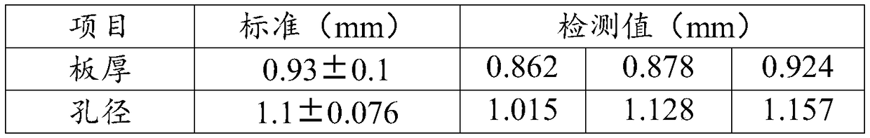
[0057] Quality data testing: Three batches of high-frequency microwave boards and high-density interconnection boards produced according to the preparation method of Example 1 were tested for finished board thickness, finished product aperture, solderability, and thermal stress. The specific test results are shown in the table 1-3.

[0058] Table 1. Test results of finished plate thickness and hole diameter

[0059]

[0060] It can be seen from Table 1 that the high-density interconnection board prepared by the present invention meets the standard requirements in parameters such as board thickness and hole diameter.

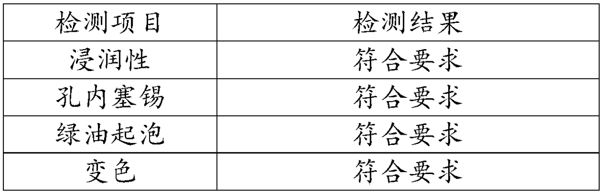
[0061] Table 2. Solderability test results

[0062]

[0063]

[0064] Among them, the test method adopts the IPC-TM-650 standard, the detection equipment adopts a tin furnace, the test temperature is 260±5°C, and the test time is 1h.

[0065] Table 3. Thermal stress test results

[0066] Test items

[0067] Among them, the test method adopts...


PUM

PropertyMeasurementUnit
thicknessaaaaaaaaaa

Abstract

A manufacture method of high-frequency microwave board high-density interconnect board relates to that technical field of high-frequency microwave product proces. A manufacture method comprises that follow steps of: cutting, Drilling, plasma degumming, Copper plating, whole plate plating, outer dry film, acid etching, Medium Inspection, Solder Resistance, silk screen printing, Electrical testing,primary product testing, Tin precipitation, secondary product testing and package, As compare with that prior art, methods of drilling, plasma processing, solder resistance and formation processes andspecific technology parameter control are optimized, and accurately controlling the time from plasma degumming slag to copper precipitation and the time from acid etching to silk screen printing, sothat the parameters of finished product such as size, surface copper, pore copper, plate thickness and pore diameter are stable, quality defects such as no copper in the pore, inhomogeneous ink thickness and the like are avoided, and the production efficiency and quality of high-frequency microwave board high-density interconnection board are improved.

Description

technical field [0001] The invention relates to the technical field of high-frequency microwave product processing, in particular to a method for manufacturing a high-density interconnection board of a high-frequency microwave board. Background technique [0002] With more and more functional requirements of electronic products, and at the same time more and more emphasis on short, small, light and thin appearance, the printed circuit board industry is also constantly developing towards high-quality and dense layout, and high-density interconnection boards are also following It came into being. High-density interconnection board is a high-precision, thin-line, small-aperture, ultra-thin printed board. It introduces blind buried holes in conventional circuit boards, fine line width and line spacing, and can manufacture conventional multi-layer board technology. Thin, multi-layer, stable circuit boards that cannot be achieved, which have the following advantages, which can re...

Claims


Application Information

Patent Timeline
Patent Type & Authority Applications(China)
IPC IPC(8): H05K3/00H05K3/06
CPCH05K3/00H05K3/0047H05K3/06H05K2203/0214H05K2203/095
Inventor 张志甲姜涛
Owner 铜陵市超远科技有限公司
Why Eureka
Try Eureka