An OLED with a micrometer periodic structure ITO electrode and a preparation method thereof

A periodic structure and electrode technology, applied in circuits, electrical components, electric solid state devices, etc., can solve the problems of difficult process technology route, low luminous efficiency, short circuit, etc., to improve the injection efficiency, increase the light output efficiency, and the process foundation is mature. Effect

Inactive Publication Date: 2019-01-18
肖和平
View PDF3 Cites 0 Cited by
  • Summary
  • Abstract
  • Description
  • Claims
  • Application Information

AI Technical Summary

Problems solved by technology

Due to the different refractive indices of OLED materials, the absorption at the organic interface and the loss of metal surface plasmon excitation mode make the light extraction efficiency of OLED about 30%. The scheme of increasing the light extraction efficiency of OLED can be roughly classified into two types: internal layer (organic active layer) and external layer (inorganic substrate surface layer) in terms of material type. The process technology route of the traditional internal layer improvement scheme is relatively difficult. And it is easy to cause problems such as short circuit and local degradation, and the processing technology of the outer layer has shortcomings such as low electron-hole injection efficiency and low luminous efficiency, which urgently need to be improved

Method used


Image

  • An OLED with a micrometer periodic structure ITO electrode and a preparation method thereof
  • An OLED with a micrometer periodic structure ITO electrode and a preparation method thereof

Examples


Embodiment Construction

[0020] The present invention will be further described below in conjunction with accompanying drawing:

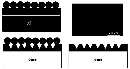
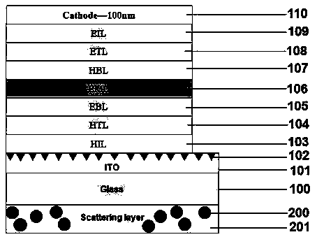
[0021] Such as Figure 1-2 As shown, a kind of OLED with micron periodic structure ITO electrode comprises glass substrate 100; Barrier layer 105, light emitting layer 106, hole blocking layer 107, electron transport layer 108, electron injection layer 109 and metal electrode layer 110; the back of the glass substrate 100 is provided with a scattering layer 200 and a curing layer 201 in sequence.

[0022] Such as Figure 1-2 As shown, a kind of OLED with micron periodic structure ITO electrode, the thickness of ITO layer 101 is 150~300nm; 107. The thickness of the electron transport layer 108, electron injection layer 109, and metal electrode layer 110 is 10-500 nm; the light-emitting layer is one of monochromatic light R, G, B or monochromatic light R, G, B The light-emitting layer composed of a combination; the metal electrode layer 110 is a combination of Al layer or ...


PUM

PropertyMeasurementUnit
Thicknessaaaaaaaaaa
Thicknessaaaaaaaaaa
Diameteraaaaaaaaaa

Abstract

The invention relates to an OLED with a micrometer periodic structure ITO electrode and a preparation method thereof, and belongs to the technical field of OLED production and manufacture. An ITO layer, a micrometer periodic structure layer, a hole injection layer, a hole transport layer, an electron barrier layer, a light emitting layer, a hole barrier layer, an electron transport layer, an electron injection layer and a metal electrode layer are sequentially arranged on the front surface of a glass substrate. A scattering layer and a curing layer are sequentially arranged on the back surfaceof the glass substrate. The OLED of the invention has novel structure and clear preparation principle, and the ITO micron periodic structure is prepared by using SiO2 micro-nano diameter ball as ICP-RIE mask complete, Prior to evaporation of the organic light-emitting layer, the surface of ITO was treated by water-gas two-fluid of H2O2 and CO2, the work function of ITO surface is increased to about 5.3 V, In order to improve the injection efficiency of electron holes, the scattering layer formed on the glass substrate is by ultraviolet curing optical adhesive (NOA73) glue and SiO2 micro-nanodiameter spheres is coated and solidified on the glass substrate. The luminescent efficiency can be improved by 10-20%. The process foundation is mature and the raw materials are easy to obtain, which is conducive to batch production.

Description

technical field [0001] The invention belongs to the technical field of OLED production and manufacture, and relates to an OLED chip structure and a process thereof, in particular to an OLED with a micron periodic structure ITO electrode and a preparation method thereof. Background technique [0002] Organic light-emitting diodes (OLEDs) have excellent image quality and are rapidly expanding in the consumer electronics market. Organic light-emitting diodes are considered to be ideal light sources for displays and lighting, but the light extraction efficiency of OLEDs lags behind III-V compound semiconductor LEDs. With the introduction of phosphorescent emitters or emitters based on thermally activated delayed fluorescence, the internal quantum efficiency of OLEDs has been greatly improved, laying the foundation for OLEDs to become ultra-efficient light-emitting diodes. Due to the different refractive indices of OLED materials, the absorption at the organic interface and the l...

Claims


Application Information

Patent Timeline
IPC IPC(8): H01L51/52H01L51/56
CPCH10K50/813H10K50/854H10K71/00
Inventor 肖和平
Owner 肖和平
Why Eureka
Try Eureka