Method for preparing non-masked P-type full back electrode contact crystalline silicon solar cell

A technology of full back electrode contact and crystalline silicon solar cells, which is applied in the field of solar cells, can solve the problems of cumbersome and complicated process and high cost, and achieve simplified preparation process, suitable for large-scale industrial application, and good conductivity Effect

Inactive Publication Date: 2019-03-22
RISEN ENERGY (CHANGZHOU) CO LTD
View PDF4 Cites 10 Cited by
  • Summary
  • Abstract
  • Description
  • Claims
  • Application Information

AI Technical Summary

Problems solved by technology

Therefore, multiple masking processes are required in the preparation process, making the process cumbersome and complicated, and the cost remains high

Method used


Image

  • Method for preparing non-masked P-type full back electrode contact crystalline silicon solar cell

Examples


Embodiment Construction

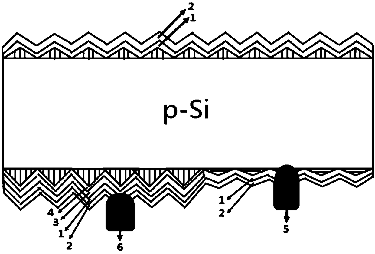
[0025] The present invention is described in further detail now in conjunction with accompanying drawing. These drawings are all simplified schematic diagrams, which only illustrate the basic structure of the present invention in a schematic manner, so they only show the configurations related to the present invention.

[0026] figure 1 It is a schematic structural diagram of a P-type full-back electrode-contact crystalline silicon solar cell without a mask in the present invention.

[0027] A method for preparing a maskless p-type full back electrode contact crystalline silicon solar cell, comprising the following steps:

[0028] (1) Texturing: Use P-type monocrystalline silicon wafers as the silicon substrate, and first perform texturing treatment. The solution used is usually KOH solution, and the KOH solution is generally based on KOH: Additive: H 2 The ratio of O=20:3:160 is prepared, and the temperature is 80°C. Then wash in 2-5% HF solution to clean the surface of th...


PUM

PropertyMeasurementUnit
thicknessaaaaaaaaaa
thicknessaaaaaaaaaa
thicknessaaaaaaaaaa

Abstract

The invention relates to the technical field of solar cells, in particular to a method for preparing a non-masked P-type full back electrode contact crystalline silicon solar cell. The method comprises the steps of: carrying out texturing; depositing tunneling silicon oxide and an intrinsic polycrystalline silicon film, and performing patterned implantation of phosphorus ions; then carrying out etching by using a TMAH solution at a concentration of 1-2% and a solution temperature of 25-80 DEG C, and etching away an intrinsic polycrystalline silicon layer in a non-n+ region and an intrinsic polycrystalline silicon layer on the front surface; then immersing the substrate in a 1-5% HF solution for 1 to 2 minutes to remove the tunneling oxide layer SiO2 in the region; then performing annealing; activating the phosphorus atoms in ion implantation to form even doping in the silicon, so as to form a pn junction region; and finally removing the phosphorosilicate glass on the surface of the pnjunction region, depositing a passivation layer, performing laser film opening, and carrying out screen printing. The method provided by the invention has the advantages of simple production process and high battery efficiency, does not have expensive processes such as boron diffusion, can greatly reduce the cost of the full back electrode contact solar cell, and is suitable for large-scale industrial application.

Description

technical field [0001] The invention relates to the technical field of solar cells, in particular to a method for preparing a P-type full-back electrode-contact crystalline silicon solar cell without a mask. Background technique [0002] IBC (Inter digitated back contact refers to interdigitated back contact) battery means that there is no electrode on the front of the battery, and the metal grid lines of the positive and negative poles are interdigitated and arranged on the back of the battery. The biggest feature of the IBC battery is that the PN junction and the metal contact are on the back of the battery, and the front is not affected by the metal electrode shielding, so it has a higher short-circuit current Jsc. At the same time, the back can allow wider metal grid lines to reduce the series resistance Rs and improve The fill factor FF; together with the front surface field (FrontSurface Field, FSF) of the battery and the open circuit voltage gain brought about by good...

Claims


Application Information

Patent Timeline
Patent Type & Authority Applications(China)
IPC IPC(8): H01L31/18H01L31/0352H01L31/0224
CPCH01L31/022441H01L31/035272H01L31/035281H01L31/1804Y02E10/547Y02P70/50
Inventor 崔艳峰袁声召万义茂黄强林海峰
Owner RISEN ENERGY (CHANGZHOU) CO LTD
Why Eureka
Try Eureka