
Color-tunable perovskite LED based on micro-nano structure and its preparation method

A technology of micro-nano structure and perovskite, which is applied in semiconductor/solid-state device manufacturing, semiconductor devices, electrical components, etc., and can solve the problem of uncontrollable color

Active Publication Date: 2020-10-20
HARBIN INST OF TECH SHENZHEN GRADUATE SCHOOL
View PDF4 Cites 0 Cited by
  • Summary
  • Abstract
  • Description
  • Claims
  • Application Information

AI Technical Summary

Problems solved by technology

[0011] Aiming at the problem that the color of the existing perovskite LED cannot be adjusted, in order to improve the adjustability of the light emission of the perovskite LED, so as to realize the free regulation of the light emission color of the perovskite LED, the present invention proposes a micro-nano structure-based adjustable Color perovskite LED and its preparation method, through the composite structure and preparation method of metal or high refractive index dielectric material micro-nano structure combined with perovskite LED, so as to obtain a new type of high brightness, high sensitivity, large color adjustment Range of Tunable Perovskite LEDs

Method used


Image

  • Color-tunable perovskite LED based on micro-nano structure and its preparation method
  • Color-tunable perovskite LED based on micro-nano structure and its preparation method
  • Color-tunable perovskite LED based on micro-nano structure and its preparation method

Examples


Embodiment 1

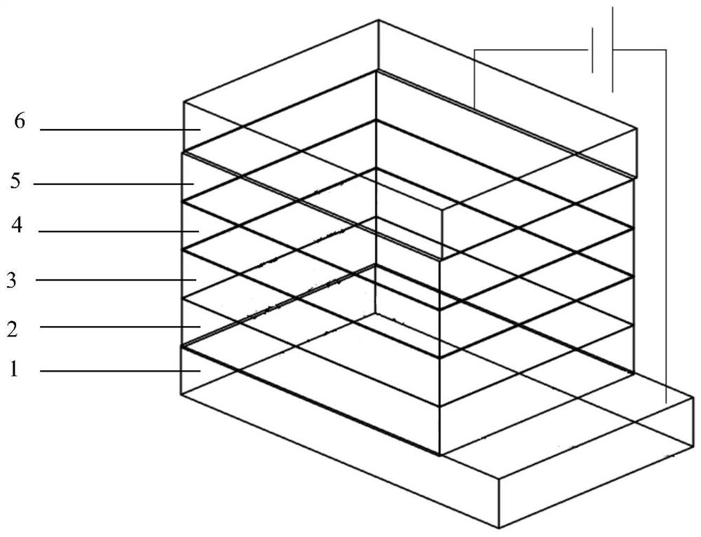
[0053] This embodiment provides an overall device structure of a color-tunable perovskite LED based on a micro-nano structure.

[0054] Such as figure 1 The overall structure of a color-tunable perovskite LED device based on micro-nano structure is shown, from bottom to top are indium tin oxide (ITO) layer 1, titanium dioxide (TiO2) layer 2, styrene sulfonate ( PEDOT:PSS) layer 3, perovskite (perovskite) layer 4, 1,3,5-tris(1-phenyl-1H-benzimidazol-2-yl)benzene (TPBi) layer 5, lithium fluoride ( LiF) / aluminum (AL) layer 6.

[0055] In terms of thickness design, the thickness of the indium tin oxide layer 1 is 13nm, the thickness of the titanium dioxide layer 2 is 230nm, the thickness of the styrene sulfonate layer 3 is 40nm, and the thickness of the perovskite layer 4 is 120nm, 1,3,5 - The thickness of the tris(1-phenyl-1H-benzimidazol-2-yl)benzene layer 5 is 40 nm, and the thickness of the lithium fluoride / aluminum layer 6 is 1 nm for the lithium fluoride layer and 100 nm ...

Embodiment 2

[0060] This embodiment provides a method for preparing the monolithic device described in Embodiment 1.

Embodiment approach

[0061] Concrete implementation scheme is as follows:

[0062] (1) Preparation of titanium dioxide layer: use a commercial 15nm thick ITO glass substrate, soak it in acetone and isopropanol in an ultrasonic cleaner for 10 minutes, take it out and dry it with clean nitrogen, and put it in the plasma Clean in a body cleaner for 10 minutes and improve the adhesion between the photoresist and the substrate. After that, a ZEP520 photoresist film with a thickness of 350nm was covered on the surface of the ITO glass substrate by spin coating, and then kept on a glue baking table at 180°C for one hour. Afterwards, the sample was subjected to pattern exposure (30kV) by an electron beam exposure system, and after taking it out, it was developed in ND510 developer solution at 0°C for 60 seconds, so that the ZEP520 photoresist formed a nanostructure. After developing and drying with clean nitrogen, the sample was transferred to the vacuum chamber of the electron beam evaporation system. A...


PUM

PropertyMeasurementUnit
thicknessaaaaaaaaaa
thicknessaaaaaaaaaa
thicknessaaaaaaaaaa

Abstract

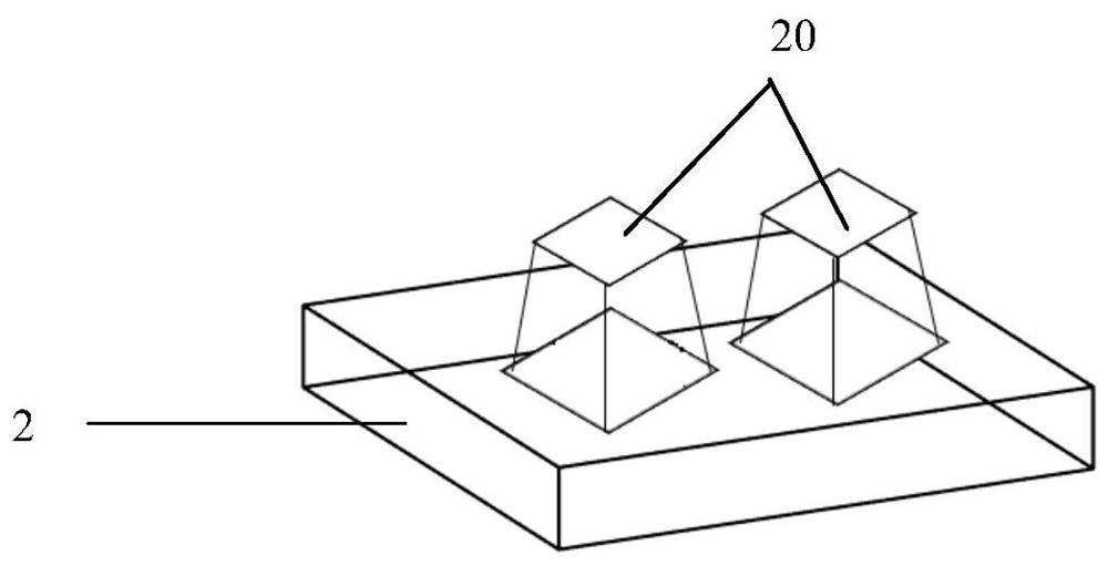
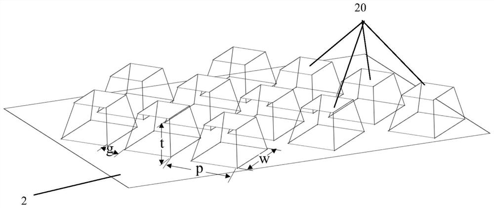
A color-tunable perovskite LED based on micro-nano structure and its preparation method. The overall device structure includes from bottom to top: indium tin oxide layer, titanium dioxide layer, styrene sulfonate layer, perovskite layer, 1 ,3,5-tris(1-phenyl-1H-benzimidazol-2-yl)benzene layer and lithium fluoride / aluminum layer, the titanium dioxide layer as a scatterer, including a plurality of monolayers and periodically arranged Titanium dioxide micro-nano structure, the longitudinal section of each titanium dioxide micro-nano structure is a trapezoid whose upper side is shorter than the lower side, the upper and lower surface cross-sections of each titanium dioxide micro-nano structure are square, and the titanium dioxide micro-nano structures are neatly arranged and formed clearly Edge, the invention also discloses a preparation method. Compared with the prior art, the present invention has simple structure, greatly simplified preparation method, high conversion efficiency and low energy consumption, and is a novel color-tunable perovskite LED with high brightness, high sensitivity and large color adjustment range.

Description

technical field [0001] The invention belongs to the field of LED photoelectric technology, in particular to a color-tunable perovskite LED based on a micro-nano structure and a preparation method thereof, which can be specifically applied to LED display screens. Background technique [0002] Perovskite LEDs have many advantages, such as direct bandgap materials, higher absorption constants, long diffusion distances, bipolar carrier transport properties, and higher defect tolerance values, etc., but perovskite LEDs only It can emit light of a specific wavelength. When the material of the perovskite layer is determined, the wavelength of the emitted light is also determined. The wavelength of the emitted light is determined by the band gap of the material. [0003] The current perovskite LED is a monochromatic light source. The existing method to change the color of the LED light is to add different elements to the perovskite layer to change its composition for color regulatio...

Claims


Application Information

Patent Timeline
Patent Type & Authority Patents(China)
IPC IPC(8): H01L51/50H01L51/56
CPCH10K50/125H10K50/00H10K71/00
Inventor 肖淑敏代振兴汪帅宋清海
Owner HARBIN INST OF TECH SHENZHEN GRADUATE SCHOOL
Learn More