IGBT device with carrier storage layer using diode clamping

A carrier storage and diode clamping technology, applied in the field of IGBT devices, can solve the problems of high saturation voltage, reduced saturation current of new IGBTs, and small short-circuit safe working area.

Active Publication Date: 2019-04-26
UNIV OF ELECTRONIC SCI & TECH OF CHINA
View PDF7 Cites 3 Cited by
  • Summary
  • Abstract
  • Description
  • Claims
  • Application Information

AI Technical Summary

Problems solved by technology

[0004] The object of the present invention is to propose a new type of gate IGBT with a carrier storage layer for the problems of high saturation voltage, small short-circuit safe working area and limited CSL concentration of the existing slot gate IGBT with a carrier storage layer. IGBT; this new type of IGBT directly integrates one or more series diodes on the surface of the silicon chip in the trench gate IGBT process to clamp the potential of the electric field shielding layer in the P region, breaking through the concentration of CSL on the basis of the existing trench gate IGBT process limit, greatly improving the injection efficiency of the IGBT emitter, thereby greatly improving the trade-off relationship between the IGBT's turn-on voltage drop and turn-off loss; at the same time, due to the clamping effect of the diode, the nMOS channel attachment of the IGBT The drain is clamped at a lower voltage under high voltage and high current, so that the saturation current of the new IGBT is greatly reduced, thereby improving the short-circuit safe working area of ​​the IGBT

Method used


Image

  • IGBT device with carrier storage layer using diode clamping
  • IGBT device with carrier storage layer using diode clamping
  • IGBT device with carrier storage layer using diode clamping

Examples


Embodiment 1

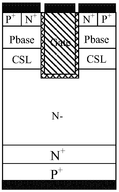
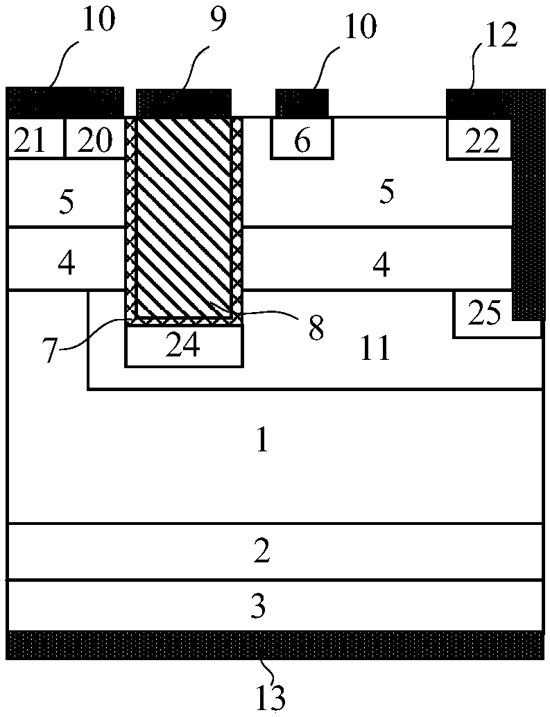
[0034] This embodiment provides an IGBT device with a carrier storage layer clamped by a diode, and its cell structure is as follows image 3 shown, including:

[0035] The voltage-resistant region 1, the N-type buffer layer 2 disposed at the bottom of the voltage-resistant region 1, the P-type collector semiconductor region 3 disposed on the lower surface of the N-type buffer layer 2, and the P-type collector semiconductor region 3 disposed on the lower surface collector metal 13;

[0036] The P-type electric field shielding layer 11 arranged on the upper surface of the withstand voltage region 1, the N-type carrier storage layer 4 covering the upper surface of the withstand voltage region 1 and the P-type electric field shielding layer 11, and the N-type carrier layer 4 covering the upper surface of the N-type electric field shielding layer 11. P-type base region 5 on the upper surface of sub-storage layer 4;

[0037] The surface of the cell is provided with a first deep g...

Embodiment 2

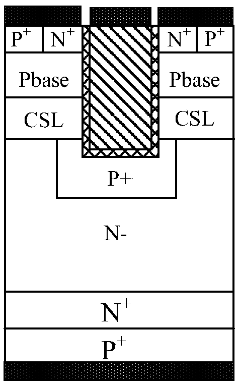
[0046] This embodiment provides a diode-clamped IGBT device with a carrier storage layer, the cell structure of which is as follows Figure 4 As shown, the difference between its cellular structure and Embodiment 1 is that: the short-circuit mode is different from Embodiment 1; in this embodiment, the P-type electric field shielding layer 11 on the other side of the first deep groove, the N-type The carrier storage layer 4 is connected to the semiconductor surface through a deep diffused P-type semiconductor region 27 and an N-type semiconductor region 28 respectively, and then the deep-diffused P-type semiconductor region 27, N-type semiconductor region 28 and the side P-type base region 5 The surface of the first P-type heavily doped semiconductor region 22 in the interior covers the metal 12; the N-type semiconductor region 28 is connected to the metal 12 through a second N-type heavily doped region 6 to form an ohmic contact; the deep diffusion P Type semiconductor region ...

Embodiment 3

[0048] This embodiment provides an IGBT device with a carrier storage layer clamped by a diode, and its cell structure is as follows Figure 5 As shown, the difference between its cell structure and that of Embodiment 1 is that n-1 N-type semiconductor isolation regions 19 are arranged in the P-type base region 5 located on the other side of the first deep groove, n≥2, and the following The surface is in contact with the N-type carrier storage layer 4, and the N-type semiconductor isolation region 19 separates the P-type base region on this side into n P-type sub-regions, and an N-type heavily doped sub-region is arranged in each P-type sub-region. The miscellaneous semiconductor region 6, the N-type heavily doped semiconductor region 6 and the respective P-type subregions form a PN junction diode, and a P-type heavily doped semiconductor region is also provided in the P-type subregion of each PN junction diode. Region 22 is used as the anode ohmic contact region of the diode,...


PUM


Abstract

The invention relates to the field of power semiconductors, provides an IGBT device with a carrier storage layer using diode clamping, and solves the problems that the saturation voltage of an existing groove gate IGBT with the carrier storage layer (CSL) is high, a short circuit safe working area is smaller, and the CSL concentration is limited. The IGBT device with the carrier storage layer using diode clamping has the advantages that the IGBT directly integrates one or more series diodes on the surface of a silicon wafer through a groove gate IGBT process for clamping electric potential ofan electric field shielding layer of a P region, on the basis of the groove gate IGBT process, the limitation of the CSL concentration is broken through, the injection efficiency of an IGBT emitting electrode is greatly improved, thereby greatly improving the tradeoff relationship between conduction voltage drop and turn-off loss of the IGBT; due to the clamping action of a diode, a drain electrode near an nMOS channel of the IGBT is clamped at a lower voltage under the high voltage and large current, so that saturation current of the novel IGBT is reduced to a great extent, thereby enlargingthe short circuit safe working area of the IGBT.

Description

technical field [0001] The invention relates to the field of power semiconductors, and provides an IGBT device with a carrier storage layer clamped by a diode, in particular an IGBT device with ultra-low conduction voltage drop, low saturation current density and fast turn-off characteristics. Background technique [0002] IGBT compromises the low turn-on voltage drop of BJT and the fast switching characteristics of MOSFET, so it is widely used in power electronic systems. [0003] The most critical characteristic of IGBT is the trade-off relationship between turn-on voltage drop and turn-off loss, as well as the safe operating area. When the IGBT is turned on, the collector injects a large number of unbalanced carriers to form a conductance modulation effect to reduce the turn-on voltage drop. When it is turned off, it takes a while for the minority carriers in the withstand voltage region to disappear, which makes the IGBT turn off slower and turn off the loss higher. In ...

Claims


Application Information

Patent Timeline
IPC IPC(8): H01L29/40H01L29/06H01L29/739H01L27/06
CPCH01L27/0629H01L29/0623H01L29/0696H01L29/402H01L29/7397H01L29/7398
Inventor 易波李平
Owner UNIV OF ELECTRONIC SCI & TECH OF CHINA
Why Eureka
Try Eureka