

Thermoelectric element, preparation method of thereof, and thermoelectric device
A thermoelectric element and thermoelectric layer technology, applied in the manufacture/processing of thermoelectric devices, thermoelectric device node lead-out materials, etc., can solve the problems of thermoelectric material matrix and barrier layer diffusion, thermoelectric device performance degradation, and affect the performance of thermoelectric materials , to achieve the effect of maintaining thermoelectric conversion efficiency and stability, high thermal conductivity and electrical conductivity, and improving service life
- Summary
- Abstract
- Description
- Claims
- Application Information
AI Technical Summary
Problems solved by technology
Method used
Image

Examples
Embodiment 1
[0048] Step 1: According to Mg 2 Ge 0.25 sn 0.73 Bi 0.02 Measure the stoichiometric ratio of each metal source (accurate to 4 decimal places), weigh the elemental elements required for the thermoelectric material according to the proportion, put them into the graphite crucible, put the graphite crucible into the quartz tube, and then evacuate to 5×10 -3 Mpa, filled with protective gas argon, and then began to smelt the sample at a current of 220A until the raw materials of each metal source melted into a liquid state. In order to ensure uniform smelting, after melting into a liquid state, it should be kept under 250A current for 1 min until a vortex is formed, then water-cooled, and then the smelted sample should be sealed. The ingot was placed in a vacuum quartz tube for annealing; the annealing temperature was 550°C and the time was 24h. The sample was then quenched with liquid nitrogen, and then the bulk sample was manually ground into a powder in a mortar to obtain Mg ...
Embodiment 2
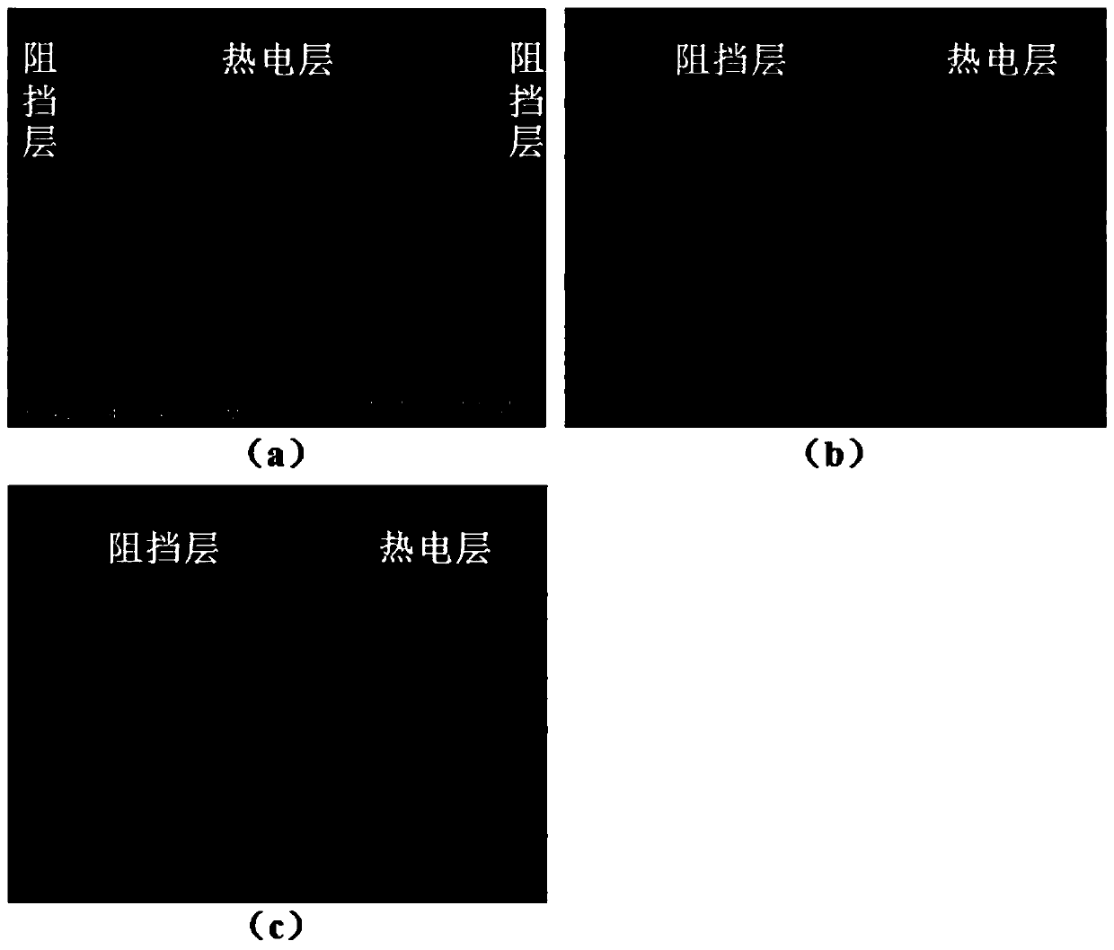
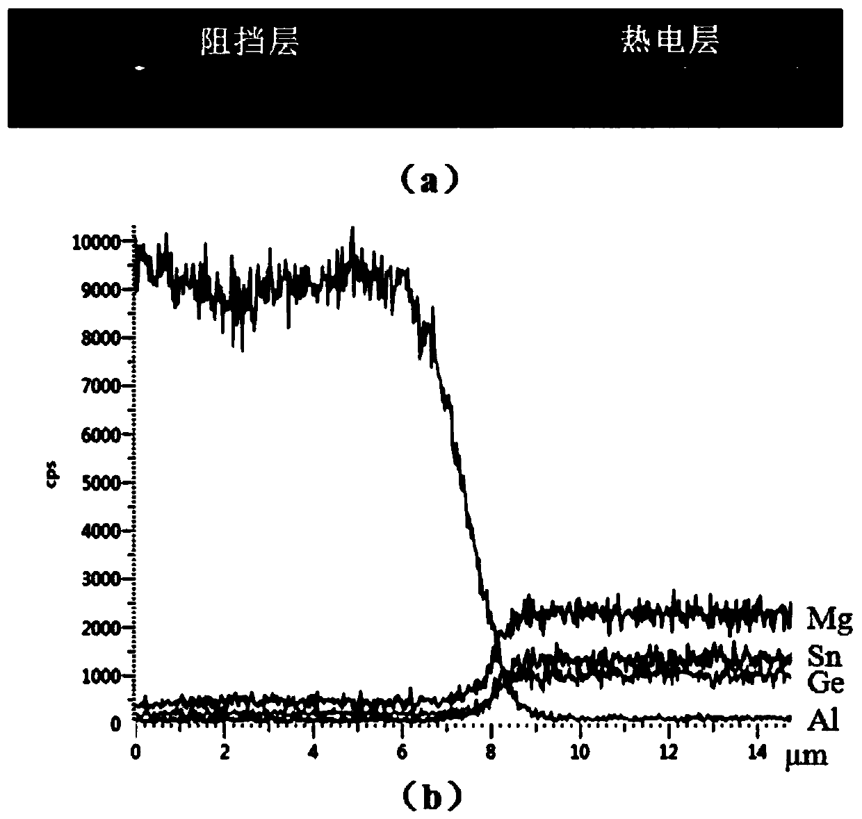
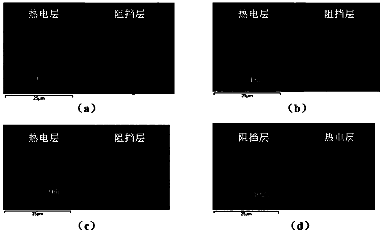
[0051] Load Mg into the graphite mold sequentially 2 Ge 0.25 sn 0.75 Powder, aluminum alloy block (containing 1% nickel), copper-nickel mixed powder, according to Mg 2 Ge 0.25 sn 0.75 The powder, the aluminum alloy block, and the copper-nickel mixed powder are loaded into the graphite mold in sequence. In a vacuum of 1.3×10 -3 MPa, the sintering pressure is 27Mpa, and the temperature is raised to 430°C at a rate of 35°C / min for SPS hot-pressing sintering for 10min, thereby producing a thermoelectric element. The thermoelectric element has Mg 2 Ge 0.25 sn 0.75 Thermoelectric layer, aluminum alloy barrier layer and copper nickel electrode layer. It was found that Mg 2 Ge 0.25 sn 0.75 The thickness of the thermoelectric layer is 8mm, the thickness of the aluminum alloy barrier layer is 0.15mm, and the thickness of the copper-nickel electrode layer is 1mm, and there are no cracks and obvious diffusion phenomena between the interfaces.
Embodiment 3
[0053] Put the silicon-germanium alloy block, aluminum sheet, and copper powder into the graphite mold in sequence, and load the silicon-germanium alloy block, aluminum sheet, and copper powder into the graphite mold in sequence. In a vacuum of 1.3×10 -3MPa, the sintering pressure is 29Mpa, and the temperature is raised to 430°C at a rate of 35°C / min for SPS hot-pressing sintering for 13min, thereby producing a thermoelectric element. The thermoelectric element has a silicon germanium alloy thermoelectric layer, an aluminum barrier layer and a copper electrode layer. After testing, it is found that there are no cracks and obvious diffusion phenomena between the interfaces.
PUM
| Property | Measurement | Unit |
|---|---|---|
| Thickness | aaaaa | aaaaa |
| Thermal expansion coefficient | aaaaa | aaaaa |
| Thickness | aaaaa | aaaaa |
Abstract
Description
Claims
Application Information