Double perovskite single crystal photodetector and preparation method thereof

A photodetector and double perovskite technology, applied in the direction of circuits, electrical components, semiconductor devices, etc., can solve the problems of restricting wide application and expansion of new technologies, inflexibility, high driving voltage, expensive manufacturing, etc., and achieve crystallization Effects of quality improvement, fast response time, and strong crystallinity

Inactive Publication Date: 2019-05-21
JINAN UNIVERSITY
View PDF5 Cites 13 Cited by
  • Summary
  • Abstract
  • Description
  • Claims
  • Application Information

AI Technical Summary

Problems solved by technology

Although photodetector fabrication processes and technologies have become mature and reliable, their complex and expensive fabrication, mechanical

Method used


Image

  • Double perovskite single crystal photodetector and preparation method thereof
  • Double perovskite single crystal photodetector and preparation method thereof
  • Double perovskite single crystal photodetector and preparation method thereof

Examples


Embodiment 1

[0040] Embodiment 1, prepare MA 1-X Cs X AgBr 6 Single-crystal perovskite photodetectors

[0041] (1) Preparation of MA 1-X Cs X AgBr 6 single crystal

[0042] The specific steps are: mix 0.0426g CsBr, 0.0449g BiBr 3 Mix and dissolve 0.0188g AgBr into 1mL of hydrobromic acid to form Cs 2 AgBr 6 solution, then add MABr to the above Cs 2 AgBr 6 In the solution until the mass concentration is 20mg / mL, heat at 140°C for 5h until the solution is clear and completely dissolved. Lower the temperature to 110°C at a rate of 2°C / h, then slowly cool down to 80°C at a rate of 1°C / h, then continue heating at 80°C for 5 hours for crystal growth to improve crystal quality, and finally quickly at a rate of 5°C / h Cool down to room temperature until MAs with a size of about 4 mm are generated 1-X Cs X AgBr 6 single crystal.

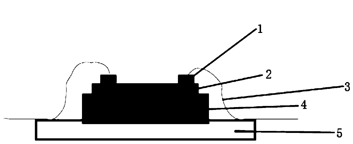
[0043] (2) MA 1-X Cs X AgBr 6 Fabrication of Single Crystal Devices

[0044] Clean the surface of the grown single crystal with isopropanol, then anneal...

Embodiment 2

[0047] Embodiment 2, preparation FA 1-X Cs X AgBr 6 Crystal Detector

[0048] According to the steps of Example 1, only the MABr used in step (1) is replaced with FABr. Then add FABr to the above Cs 2 AgBr 6 solution until the mass concentration is 20mg / mL.

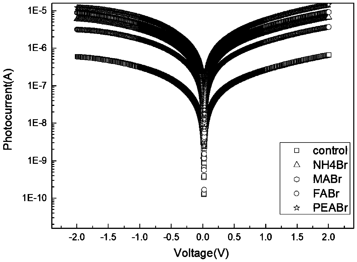
[0049] Apply a bias voltage from -2V to 2V to the single crystal device, respectively in the dark state and 1000W / m 2 Under the light intensity, test its current. It is found that the difference between its bright and dark currents is more than 3 orders of magnitude. Specifically, at 1V, its dark current is 1.49×10 -9 A, its photocurrent is 1.49×10 -6 a.

Embodiment 3

[0050] Embodiment 3, preparation PEA 1-X Cs X AgBr 6 Crystal Detector

[0051] According to the steps of Example 1, only the MABr used in step (1) was replaced with PEABr. Then add PEABr to the above Cs 2 AgBr 6 solution until the mass concentration is 20mg / mL. Apply a bias voltage from -2V to 2V to the single crystal device, respectively in the dark state and 1000W / m 2 Under the light intensity, test its current. It is found that the difference between its bright and dark currents is more than 4 orders of magnitude. Specifically, at 1V, its dark current is 5.76×10 -10 A, its photocurrent is 5.76×10 -6 a.


PUM

PropertyMeasurementUnit
Thicknessaaaaaaaaaa

Abstract

The invention discloses a double perovskite single crystal photodetector and a preparation method thereof. The double perovskite single crystal photodetector comprises a substrate, wherein the substrate is provided with a double perovskite single crystal, electrodes and a silver glue in sequence, the two electrodes are respectively connected to a conductive gold wire, the double perovskite singlecrystal is in a double perovskite structure formed by adding different cations in a solution of the perovskite growth single crystal, and each of the added cations is one of methylamine ion (MA+), formamidine ion (FA+), phenethylamine ion (PEA+), NH4+, butylamine ion (Ba+), K+, Rb+ and Tl+. By doping different cations in the double perovskite single crystal photodetector, the carrier concentrationof the device is increased under illumination conditions, which leads to an increase in photocurrent and enhances the detection performance of the photodetector.

Description

technical field [0001] The invention belongs to the field of perovskite photoelectric detectors, and relates to a double perovskite single crystal photoelectric detector and a preparation method thereof. Background technique [0002] In recent years, a photodetector is a device for detecting and measuring the properties of light through the photoelectric effect, which usually manifests itself as a photocurrent. Nowadays, photoelectric conversion on photodetectors has attracted increasing attention in both academic and industrial fields for a wide range of applications such as image sensing, optical communication, environmental monitoring, chemical detection, and biological detection. Semiconductor materials are essential to absorb incident photons and generate electron-hole pairs upon photoexcitation. A built-in or applied electric field is also necessary to separate electrons and holes to generate an electric current. The main photodetectors are made of inorganic semicond...

Claims


Application Information

Patent Timeline
IPC IPC(8): H01L31/032H01L31/18
CPCY02P70/50
Inventor 范建东李闻哲袁伟南王华民麦耀华
Owner JINAN UNIVERSITY
Why Eureka
Try Eureka