Composite nano cold cathode structure with high stability electron emission and preparation method
A technology of electron emission and cold cathode, which is applied in cold cathode manufacturing, electrode system manufacturing, discharge tube/lamp manufacturing, etc. It can solve problems such as melting point limitation and electric field change, and achieve low turn-on electric field, simple structure, and high stability. The effect of electron emission
- Summary
- Abstract
- Description
- Claims
- Application Information
AI Technical Summary
Problems solved by technology
Method used
Image

Examples
Embodiment 1
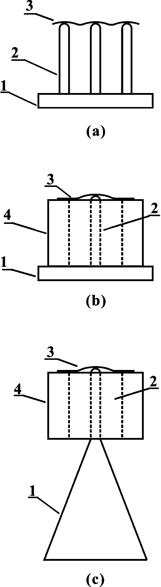
[0035] Such as figure 1 As shown, the structural schematic diagrams of three composite low-dimensional nano-cold cathodes using nanowires as low-dimensional cold cathode materials on the basis of different substrates are given.
[0036] The basic structure of the cold cathode includes a substrate 1 , a low-dimensional nano cold cathode 2 , a two-dimensional film material 3 and a support structure 4 .
[0037] figure 1 In a, the substrate 1 is a planar structure, and the supporting structure is the low-dimensional nano cold cathode array itself; figure 1 In b, the substrate 1 is a planar structure, and the supporting structure is an integrated small hole in the insulating layer; figure 1 In c, the substrate 1 is a tapered structure, and the supporting structure is a separated ceramic mesh / copper mesh.
Embodiment 2
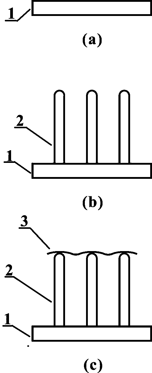
[0039] based on figure 1 Schematic diagram of the fabrication process of the composite nano-cold cathode structure.
[0040] Such as figure 2 as shown, figure 2 given in Example 1 figure 1 Fabrication flowchart of the composite nano-cold cathode structure in a. First prepare a flat substrate 1 ( figure 2 a); Then, vertical and equal-height low-dimensional nano-cold cathodes 2 are prepared on it, and multiple low-dimensional nano-cold cathodes 2 form a low-dimensional nano-cold cathode array ( figure 2 b); Finally, the two-dimensional thin film material 3 is transferred to the low-dimensional nano cold cathode 2 ( figure 2 c). The equal-height low-dimensional nano-cold cathode ensures that the geometric curvature of the tip of the two-dimensional film material is smaller than that of the tip of the nanowire.
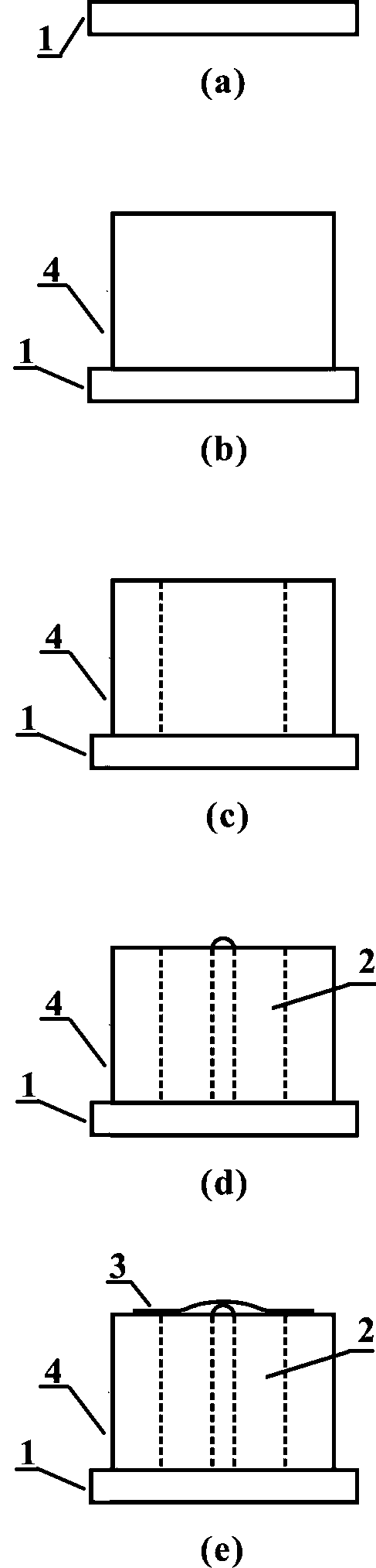
[0041] Such as image 3 as shown, image 3 given in Example 1 figure 1 Fabrication flowchart of the composite nano-cold cathode structure in b. First prep...
Embodiment 3
[0045] Figure 5 It is the simulation result of the surface energy band bending of the compound low-dimensional nano-cold cathode whose tip curvature of the two-dimensional thin film material is larger / smaller than that of the low-dimensional nanostructure tip.
[0046] Such as Figure 5 a and Figure 5 As shown in b, the schematic diagrams of the structures in which the geometric curvature of the tip of the two-dimensional thin film material is greater than and smaller than that of the nanowire tip are respectively listed. According to geometry, Figure 5 The 2D thin film material in b is in close contact with the nanowire tip at the tip, while Figure 5 The two-dimensional thin film material in a forms a suspended structure at the tip.
[0047] Figure 6 It is the simulation result of the surface energy band bending of single-layer tungsten diselenide films with different thicknesses under the applied electric field of 2.5 V / nm; Band bending under nm electric field. i...
PUM
| Property | Measurement | Unit |
|---|---|---|
| thickness | aaaaa | aaaaa |
Abstract
Description
Claims
Application Information
 - R&D
- Intellectual Property
- Life Sciences
- Materials
- Tech Scout
- Unparalleled Data Quality
- Higher Quality Content
- 60% Fewer Hallucinations
Browse by: Latest US Patents, China's latest patents, Technical Efficacy Thesaurus, Application Domain, Technology Topic, Popular Technical Reports.
© 2025 PatSnap. All rights reserved.Legal|Privacy policy|Modern Slavery Act Transparency Statement|Sitemap|About US| Contact US: help@patsnap.com