Chip stack stereoscopic package structure and manufacturing method thereof
A technology of three-dimensional packaging and chip stacking, which is applied in semiconductor/solid-state device manufacturing, electric solid-state devices, semiconductor devices, etc., can solve the problems that affect the overall yield rate of the stacked packaging structure, low wafer yield rate, cost loss, etc., and achieve improvement The effects of signal quality, improved bonding efficiency, and reduced production costs
- Summary
- Abstract
- Description
- Claims
- Application Information
AI Technical Summary
Problems solved by technology
Method used
Image

Examples
Embodiment approach 1
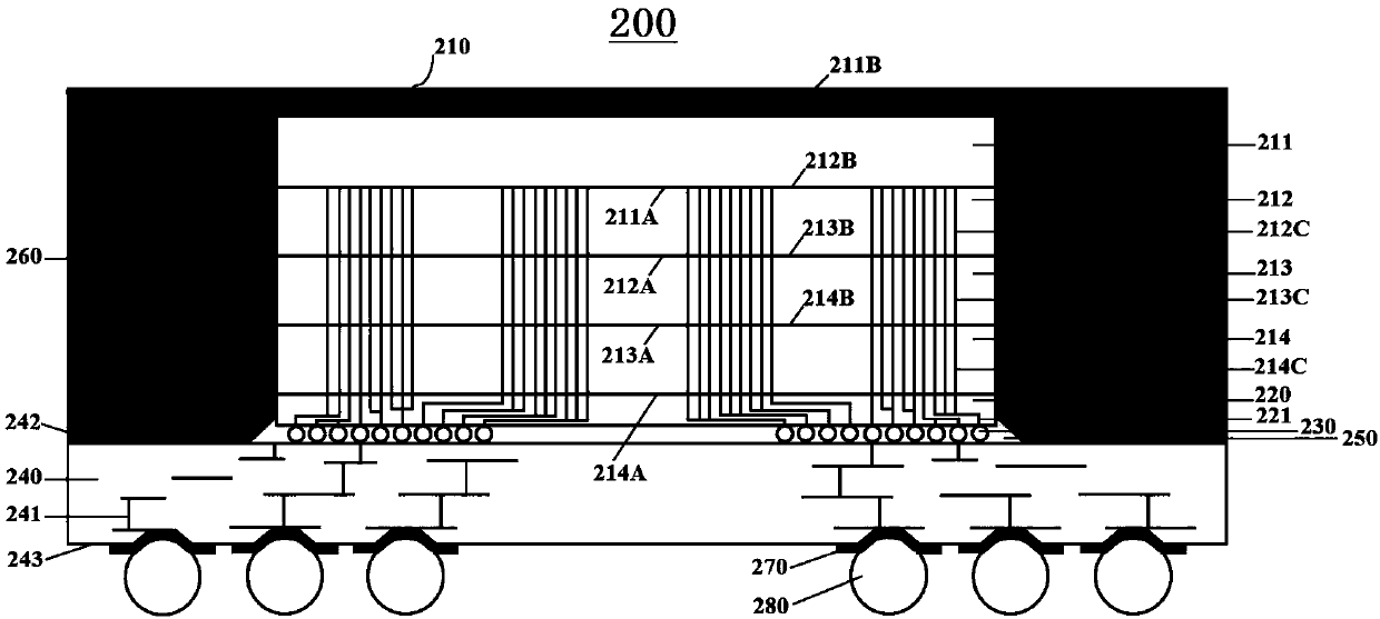
[0109] figure 2 It is a schematic diagram of the chip stack three-dimensional package structure provided by an embodiment of the present invention. Such as figure 2 As shown, the three-dimensional chip stack package structure 200 according to the embodiment of the present invention includes: a chip stack body 210, a first redistribution layer 220, flip-chip terminals 230, a substrate 240, a primer 250, a plastic package body 260, and a second metal pad 270 , External terminal 280. Wherein, the chip stack 210 includes: a top chip 211, a second chip 212, a first chip 213 and a bottom chip 214; the top chip 211 has a top active surface 211A and a crystal back 211B opposite to the top active surface 211A; The first chip 213 has a first active surface 213A and a stack back surface 213B opposite to the first active surface 213A, and the bottom chip 214 has a mounting surface 214A and The stack back 214B opposite to the mounting surface 214A; the active surface of each chip and ...
Embodiment approach 2
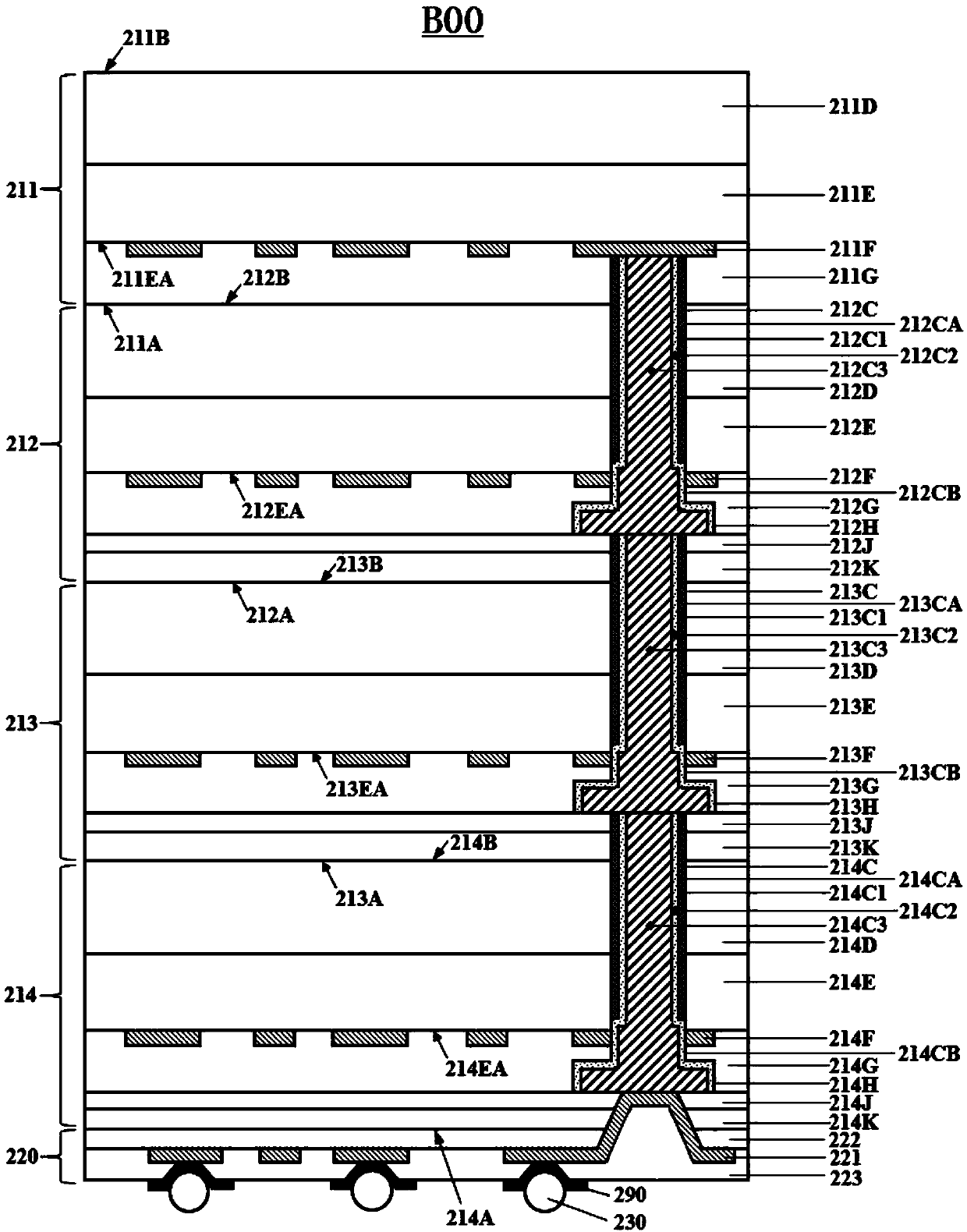
[0130] figure 2 In the chip stack three-dimensional packaging structure shown, the bottom chip 214 can be a different chip from the top chip 211, the second chip 212 and the first chip 213, such as Figure 4 shown. In some embodiments, the top chip 211 , the second chip 212 and the first chip 213 are memory chips, such as DRAM (Dynamic Random Access Memory, Dynamic Random Access Memory) chips, and the bottom chip 214 is a buffer chip. The buffer chip is to separate the circuit used to control data transmission in the memory chip and set it as an independent control chip, and it is made by using a process different from that of the memory chip. Its response speed is much higher than that of the memory chip to improve data transmission. transfer speed.
[0131] It should be noted that although the bottom chip 214 is different from the top chip 211 , the second chip 212 and the first chip 213 , the structure of the bottom chip 214 is the same as that of the second chip 212 and...
Embodiment approach 3、4
[0133] figure 2 and Figure 4 The chip stack three-dimensional packaging structure shown can also only stack three layers of chips, and the specific structures are as follows: Figure 5 and Figure 6 shown. Figure 5 implementation of Figure 6 The implementation of the differs in that Figure 5 The bottom chip 214 in is the same chip as the top chip 211 and the first chip 213, while Figure 6 The bottom chip 314 in is a different chip from the top chip 211 and the first chip 213 Figure 5 and Figure 6 respectively with figure 2 and Figure 4 Descriptions of the same parts shown can be found in the figure 2 and Figure 4 description and will not be repeated here.
PUM
 Abstract
Description
Claims
Application Information