Gas-sensitive membrane and preparation method and application thereof

A gas-sensing film and single-layer technology, applied in the field of gas-sensing sensors, can solve the problems of not greatly improving gas-sensing performance, poor gas-sensing performance, and increased specific surface area, achieving good application prospects, improving performance consistency, Good batch stability

Inactive Publication Date: 2019-05-28
INST OF PROCESS ENG CHINESE ACAD OF SCI
View PDF5 Cites 9 Cited by
  • Summary
  • Abstract
  • Description
  • Claims
  • Application Information

AI Technical Summary

Problems solved by technology

Although there are also many research attempts to use MEMS coating methods such as sputtering to make gas-sensitive thin films (such as CN1888123A, Thin Solid Films 516 (2008) 5111-5117), the thin films made by traditional sputtering methods are usually relatively dense and interact with gases. The specific surface area is small, and the gas sensitivity performance is poor
There are also studies that try to use post-annealing and other processes to sinter the sputtered film into a porous film at high temperature (Sensors and Actuators B 24-25 (1995) 433-437), but the increase in specific surface area is limited, and its gas-sensing performance has not been greatly improved.

Method used


Image

  • Gas-sensitive membrane and preparation method and application thereof
  • Gas-sensitive membrane and preparation method and application thereof

Examples


Embodiment 1

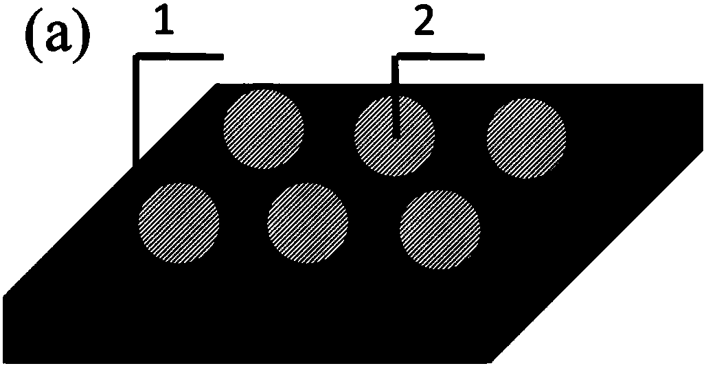
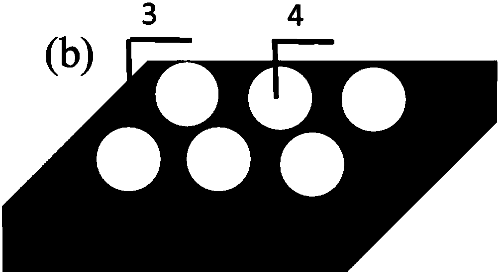
[0048] (1) The sensor substrate is made by conventional technology, including Si 3 N 4 / Si substrate cleaning, fabrication of Pt heating resistors by photolithography, deposition of insulating layers such as silicon oxide or aluminum oxide, fabrication of gold finger electrodes by photolithography, and exposure of the gold finger electrode area through conventional photolithography processes.

[0049] (2) Then spread polystyrene (PS) microspheres with a diameter of 500nm on the water surface. Due to the repulsion between the microspheres, a self-assembled microsphere layer will float on the water surface. The single-layer PS sphere was picked up from the water surface with the sensor substrate wafer, dried and put into the magnetron sputtering apparatus. Sputtering SnO with a power of 100W 2 / Pd target for 30 minutes to obtain SnO with a thickness of about 100nm 2 film.

[0050] (3) Finally, soak the wafer in a chloroform solvent for half an hour to remove the PS microsphe...

Embodiment 2

[0053] (1) The sensor substrate is made by conventional technology, including Si 3 N 4 / Si substrate cleaning, fabrication of Pt heating resistors by photolithography, deposition of insulating layers such as silicon oxide or aluminum oxide, fabrication of gold finger electrodes by photolithography, and exposure of the gold finger electrode area through conventional photolithography processes.

[0054] (2) Then spread the polyacrylate microspheres with a diameter of 2000nm on the water surface. Due to the repulsion between the microspheres, a self-assembled microsphere layer will float on the water surface. The single-layer polyacrylate microspheres were picked up from the water surface with the sensor substrate wafer, dried and put into the magnetron sputtering apparatus. Using 120W of power to sputter WO 3 Target for 50 minutes to obtain WO with a thickness of about 500nm 3 film.

[0055] (3) Finally, place the film in a muffle furnace to raise the temperature to 500° C. ...

Embodiment 3

[0058] In addition to replacing the diameter of polystyrene (PS) microspheres with 8000nm, and sputtering SnO with a thickness of about 100nm 2 Except that the thin film is replaced by sputtering 800nm ​​ZnO, other preparation methods and conditions are the same as in Example 1.

[0059] The yield rate of the methane sensor obtained in this embodiment is >95%, and the consistency deviation is <10%.


PUM

PropertyMeasurementUnit
diameteraaaaaaaaaa
thicknessaaaaaaaaaa
diameteraaaaaaaaaa

Abstract

The invention relates to a gas-sensitive membrane and a preparation method and application thereof. The gas-sensitive membrane is a single-layer porous mesh gas-sensitive membrane. The method is a mask sputtering method and specifically comprises the steps that a single layer of organic microspheres is flatly laid on a whole sensor substrate to serve as a mask plate, then an oxide gas-sensitive thin film is deposited, and finally the single-layer organic microsphere mask plate is removed to obtain the single-layer porous gas-sensitive membrane. According to the method, a gas-sensitive sensor wafer of a suspended structure can be further obtained by adopting a traditional back etching process, and laser cutting and splitting packaging are adopted to obtain a gas-sensitive sensor device. According to the method, a traditional dense two-dimensional thin film is cut into a porous net structure, the specific surface area is large, the porosity is increased, the interaction area between thethin film and gas is increased, and then the sensitivity is improved. Meanwhile, the gas-sensitive membrane prepared through the sputtering method is consistent in performance and relatively good in batch stability and has good application prospects.

Description

technical field [0001] The invention belongs to the field of gas-sensitive sensors, and relates to a gas-sensitive film, its preparation method and application, in particular to a single-layer porous mesh gas-sensitive film, its mask sputtering preparation method and its application in gas-sensitive sensor devices. Background technique [0002] Due to the advantages of small size, low cost, and fast response, oxide semiconductor gas sensors are widely used in the fields of flammable gas leakage and detection of toxic and harmful gas concentrations. The traditional fabrication method of oxide semiconductor gas sensors is to coat or print synthetic gas-sensitive materials on the sensor substrate, where the substrate includes a ceramic tube with a heating wire in the middle or a flat substrate with a heating plate printed on the back. Gas sensors based on traditional substrates have large volume and high power consumption. Therefore, in recent years, the substrate of the gas s...

Claims


Application Information

Patent Timeline
Patent Type & Authority Applications(China)
IPC IPC(8): G01N27/12
Inventor 韩宁王颖周新愿陈运法
Owner INST OF PROCESS ENG CHINESE ACAD OF SCI
Why Eureka
Try Eureka