Mold for growth of transistor through heat exchange method and growth method of transistor by using mold

A heat exchange method and transistor technology, applied in the direction of single crystal growth, crystal growth, single crystal growth, etc., can solve the problem of low utilization rate of crystal materials, and achieve the effects of saving manpower, smooth surface and regular appearance

Pending Publication Date: 2019-06-07
NANJING TONGLI CRYSTAL MATERIALS RES INST CO LTD
View PDF9 Cites 0 Cited by
  • Summary
  • Abstract
  • Description
  • Claims
  • Application Information

AI Technical Summary

Problems solved by technology

[0004] The purpose of the present invention is to solve the problems of traditional processing methods in the prior art and the low utilization rate of crystal materials, etc., and improve it. It relates to a mold with the advantages of simple structure and easy processing, which can grow different types of transistors.

Method used


Image

  • Mold for growth of transistor through heat exchange method and growth method of transistor by using mold

Examples


Embodiment 1

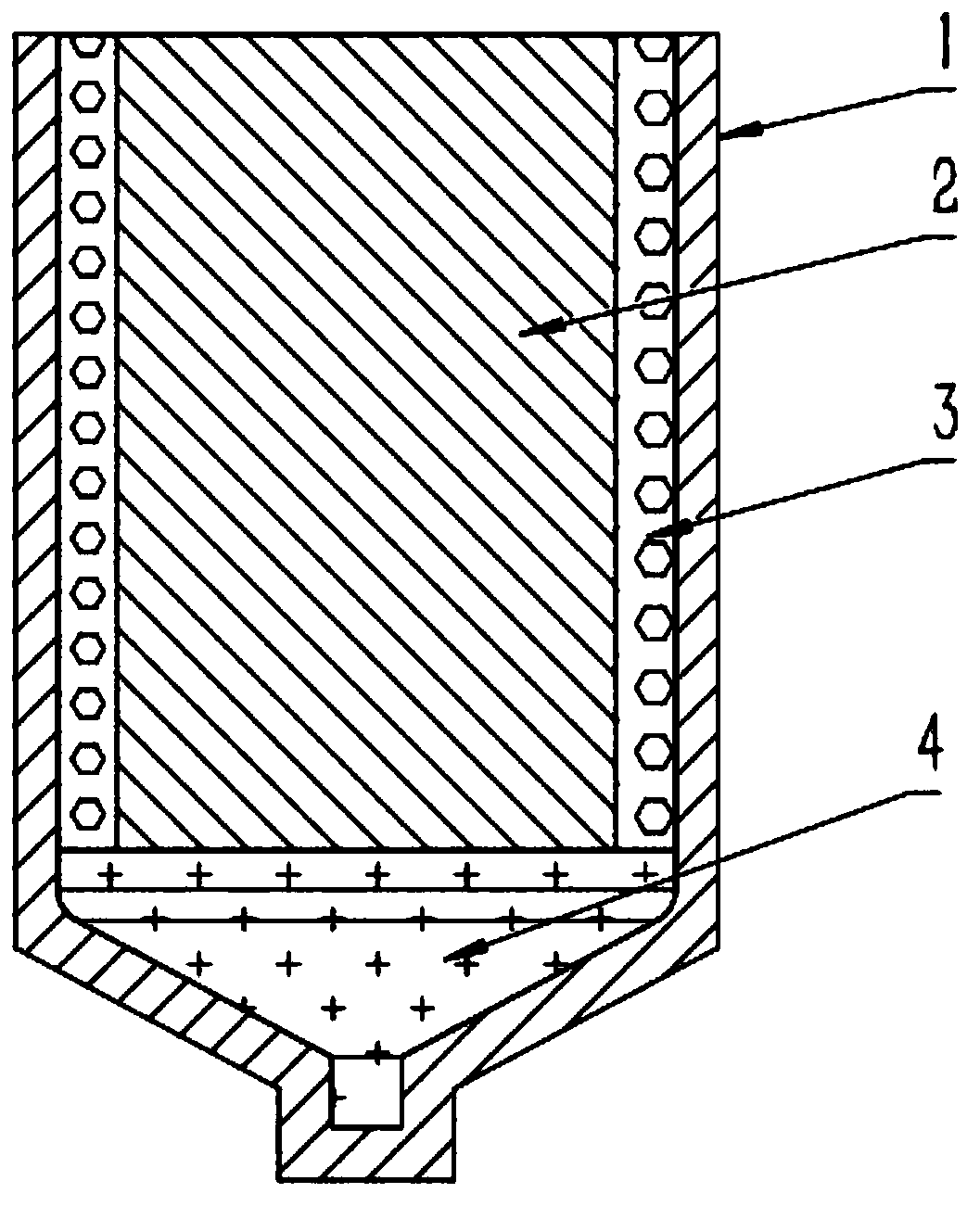
[0038] The inner diameter of the crucible 1 used is 200 mm, the diameter of the cylinder 2 is 190 mm, and the height is 260 mm.

[0039] S01, first the seed crystal area 4 is loaded into Y 3 Al 5 o 12 (YAG) seed crystal; loaded into cylinder 2 above; according to Y 3 Al 5 o 12 Chemical formula, weigh Y in proportion 2 o 3 、Al 2 o 3 High-purity raw materials are fully mixed and loaded into the transistor growth area 3;

[0040] S02, vacuumize, and pass inert gas as a protective atmosphere;

[0041] S03, raise the temperature until the raw material is completely melted, heat treatment at constant temperature for 17 hours, and control the seed crystal not to melt by controlling the power and the rate of feeding inert gas;

[0042] S04, slowly lower the temperature at 0.5-1.0°C / h to crystallize the melt in the mold from bottom to top;

[0043] S05, after the growth of the transistor is completed, drop to a certain temperature at 1.5-2.2°C / h to complete the annealing pro...

Embodiment 2

[0046] The inner diameter of the crucible 1 used is 100 mm, the diameter of the cylinder 2 is 80 mm, and the height is 260 mm.

[0047] S01, first load the sapphire seed crystal in the seed crystal area 4; install the above-mentioned cylinder 2; weigh the Al 2 o 3 High-purity raw materials are loaded into the transistor growth area 3;

[0048] S02, vacuumize, and pass inert gas as a protective atmosphere;

[0049] S03, raise the temperature until the raw material is completely melted, heat treatment at constant temperature for 15 hours, and control the seed crystal not to melt by controlling the power and the rate of feeding inert gas;

[0050] S04, slowly lower the temperature at 0.5-1.0°C / h to crystallize the melt in the mold from bottom to top;

[0051] S05, after the growth of the transistor is completed, drop to a certain temperature at 1.5-3.0°C / h to complete the annealing process;

[0052] S06, cooling down to room temperature at a cooling rate of 25-30° C. / h, takin...

Embodiment 3

[0054] The inner diameter of the crucible 1 used is 50 mm, the diameter of the cylinder 2 is 20 mm, and the height is 270 mm.

[0055] S01, first load the sapphire seed crystal in the seed crystal area 4; install the above-mentioned cylinder 2; weigh the Al 2 o 3 High-purity raw materials are loaded into the transistor growth area 3;

[0056] S02, vacuumize, and pass inert gas as a protective atmosphere;

[0057] S03, heat up until the raw material is completely melted, heat treatment at constant temperature for 8 hours, and control the seed crystal not to melt by controlling the power and the rate of feeding inert gas;

[0058] S04, slowly lower the temperature at 0.6-0.8°C / h, so that the melt in the mold crystallizes from bottom to top;

[0059] S05, after the growth of the transistor is completed, drop to a certain temperature at 2.5-3.0°C / h to complete the annealing process;

[0060] S06, cooling down to room temperature at a cooling rate of 10-30° C. / h, taking out the...


PUM

PropertyMeasurementUnit
diameteraaaaaaaaaa
heightaaaaaaaaaa
diameteraaaaaaaaaa

Abstract

The invention provides a mold for growth of a transistor through a heat exchange method and a growth method of the transistor by using the mold. The mold is a crucible of an inverted convex-shaped hollow cylindrical structure, wherein the bottom of the crucible is a seed crystal region, the upper end is a transistor growth region and a cylinder, and the cylinder is disposed in the middle of the entire structure along the center axis of the crucible; and the transistor growth region is disposed between the cylinder and the crucible, and the cylinder is detachably mounted in the crucible. The growth method of the transistor comprises the steps: performing furnace loading, performing vacuuming, introducing shielding gas, performing heating for material melting, performing transistor growth, performing annealing, taking out the transistor, and controlling the heating power and the flow rate of the shielding gas so as to control the temperature change and the environment in a furnace. Whenthe growth method is compared with a conventional processing technology, direct growth is performed on the transistor by using the heat exchange method, the crystal utilization rate can be improved effectively, and the production cost is reduced; and the size of the transistor is controllable, and the processing procedures are simplified.

Description

technical field [0001] The invention belongs to the field of crystal growth, in particular to a mold and a growth method for growing a transistor by a heat exchange method. Background technique [0002] Compared with glass and ceramics, crystals have many excellent characteristics, such as stable physical and chemical properties, good thermal properties, and high optical and electrical properties. They can be made into a variety of key materials with special properties and are widely used. In particular, sapphire single crystal has become an ideal mid-infrared window material due to its relatively superior comprehensive properties, and has been widely used in military optoelectronic equipment. Moreover, it has extremely high hardness and extremely low friction coefficient, second only to diamond; it has excellent spectral transmission performance in the ultra-wide band; and, sapphire single crystal has strong resistance to acid and alkali corrosion. It cannot be eroded even...

Claims


Application Information

Patent Timeline
Patent Type & Authority Applications(China)
IPC IPC(8): C30B11/00C30B33/02C30B29/20
Inventor 薛艳艳徐军吴锋徐晓东李东振王东海王庆国
Owner NANJING TONGLI CRYSTAL MATERIALS RES INST CO LTD
Why Eureka
Try Eureka