Preparation method of trench MOSFET integrating Schottky diode

A technology of Schottky diodes and trenches, which is applied in the direction of electrical components, electric solid devices, circuits, etc., can solve the problems of asymmetric sidewall technology, which is difficult to realize, large forward conduction loss recovery current, and low product yield. , to achieve the effect of improving device performance, improving yield level, and reducing manufacturing difficulty

Inactive Publication Date: 2019-06-18
JIANGSU HAIDONG SEMICON TECH CO LTD
View PDF5 Cites 6 Cited by
  • Summary
  • Abstract
  • Description
  • Claims
  • Application Information

AI Technical Summary

Problems solved by technology

P-N junction diodes have undesirable characteristics in operation: huge forward conduction losses, charge storage between bulk-epitaxial junction in forward configuration, when power MOSFET is switched from forward bias to reverse bias Excessive storage of minority carrier charges leads to huge recovery current and voltage overshoot, as well as switch node voltage overshoot and ringing in DC-DC conversion applications. Chinese patent CN201210138850.9 proposes a solution to the shortcomings of the previous technology, but now The asymmetric sidewall process in the existing technology is difficult and difficult to realize, and the product yield is low, so further improvement is needed

Method used


Image

  • Preparation method of trench MOSFET integrating Schottky diode
  • Preparation method of trench MOSFET integrating Schottky diode
  • Preparation method of trench MOSFET integrating Schottky diode

Examples


Embodiment 1

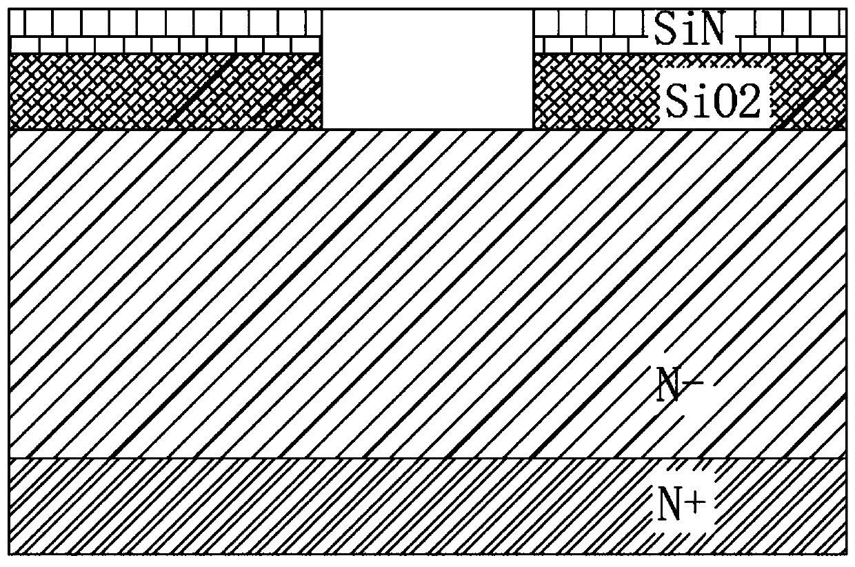
[0025] The present invention is explained by taking N-channel devices as an example, and P-channel devices can also be prepared by a similar process. figure 1 In this case, the N-type substrate 101 (N- epitaxial layer grown on the N++ substrate) is used as the drain of the device. In this example, the doping concentration of the epitaxial layer is 5.15×10 15 / cm 3 , the thickness is 7um.

[0026] S1: combine figure 1 , a silicon dioxide layer is formed on the N-region by deposition or thermal oxidation, and a silicon nitride layer is deposited on top of the silicon dioxide layer. In this example, the thickness of the silicon dioxide layer is The thickness of the silicon nitride layer is The oxide layer needs to have a certain thickness to prevent contamination of the source region during the subsequent preparation of the Schottky region.

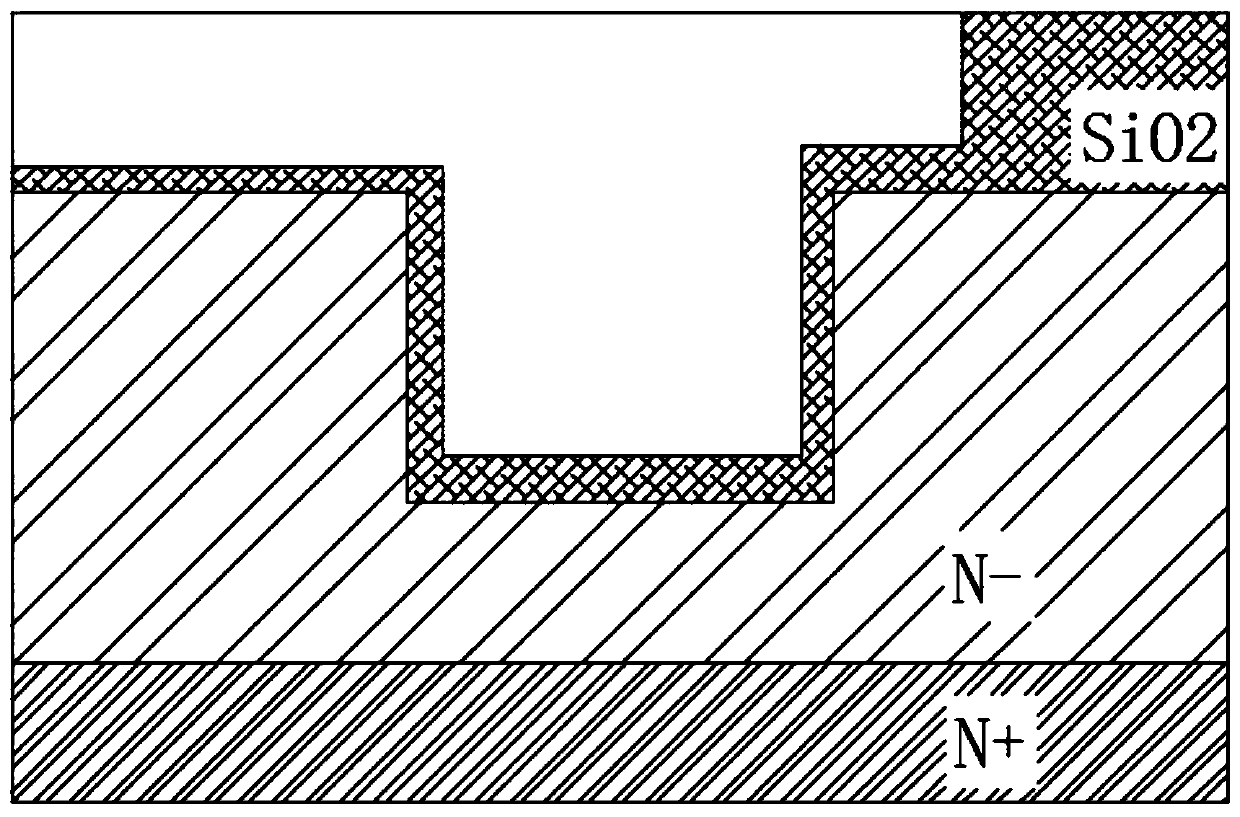
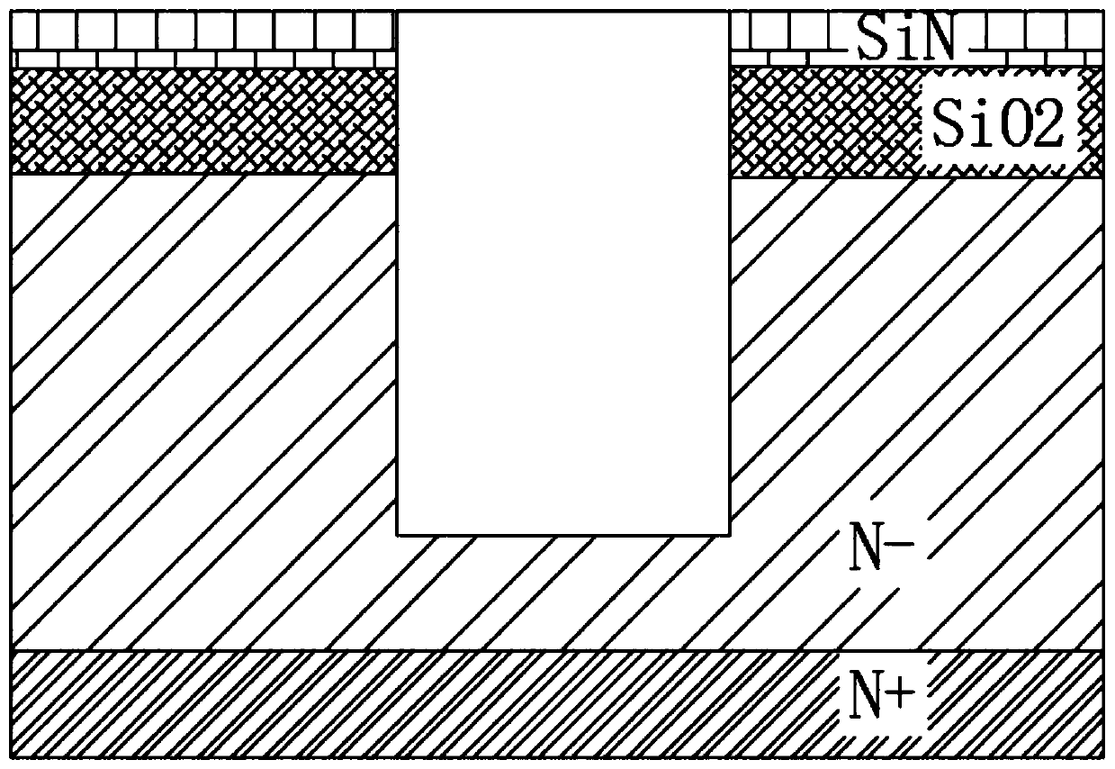
[0027] S2: combine figure 2 , apply photoresist on the silicon nitride layer, and use the first layer of mask plate, using the char...

Embodiment 2

[0036] The present invention is explained by taking N-channel devices as an example, and P-channel devices can also be prepared by a similar process. figure 1 In this case, the N-type substrate 101 (N- epitaxial layer grown on the N++ substrate) is used as the drain of the device. In this example, the doping concentration of the epitaxial layer is 5.15×10 15 / cm 3 , the thickness is 7um.

[0037] S1: combine figure 1 , a silicon dioxide layer is formed on the N-region by deposition or thermal oxidation, and a silicon nitride layer is deposited on top of the silicon dioxide layer. In this example, the thickness of the silicon dioxide layer is The thickness of the silicon nitride layer is The oxide layer needs to have a certain thickness to prevent contamination of the source region during the subsequent preparation of the Schottky region.

[0038] S2: combine figure 2 , apply photoresist on the silicon nitride layer, and use the first layer of mask plate, using the char...

Embodiment 3

[0047] The present invention is explained by taking N-channel devices as an example, and P-channel devices can also be prepared by a similar process. figure 1 In this case, the N-type substrate 101 (N- epitaxial layer grown on the N++ substrate) is used as the drain of the device. In this example, the doping concentration of the epitaxial layer is 5.15×10 15 / cm 3 , the thickness is 7um.

[0048] S1: combine figure 1 , a silicon dioxide layer is formed on the N-region by deposition or thermal oxidation, and a silicon nitride layer is deposited on top of the silicon dioxide layer. In this example, the thickness of the silicon dioxide layer is The thickness of the silicon nitride layer is The oxide layer needs to have a certain thickness to prevent contamination of the source region during the subsequent preparation of the Schottky region.

[0049] S2: combine figure 2 , apply photoresist on the silicon nitride layer, and use the first layer of mask plate, using the char...


PUM


Abstract

The invention discloses a preparation method of a trench MOSFET integrating a Schottky diode. The method comprises the steps of first, trench construction; second, conductive region preparation; third, conductive trench arrangement; fourth, Schottky structure activation; and fifth, conductive lead preparation. According to the embodiment, the structure of a power MOSFET device integrating the Schottky diode function is provided; and even though the Schottky diode is integrated in the MOSFET structure, through optimization of structural design and layout design, the manufacturing difficulty inpractical production is lowered, the yield of the device is improved, cost is lowered, and device performance is improved.

Description

technical field [0001] The invention relates to the technical field of Schottky diode preparation, in particular to a preparation method of a trench MOSFET integrating a Schottky diode. Background technique [0002] The Schottky diode is named after its inventor, Dr. Schottky, and SBD is the abbreviation of Schottky Barrier Diode (Schottky Barrier Diode, abbreviated as SBD). SBD is not made by using the principle of contacting P-type semiconductor and N-type semiconductor to form PN junction, but using the principle of metal-semiconductor junction formed by contacting metal and semiconductor. Therefore, SBD is also called metal-semiconductor (contact) diode or surface barrier diode, which is a kind of hot carrier diode. P-N junction diodes have undesirable characteristics in operation: huge forward conduction losses, charge storage between bulk-epitaxial junction in forward configuration, when power MOSFET is switched from forward bias to reverse bias Excessive storage of ...

Claims


Application Information

Patent Timeline
Patent Type & Authority Applications(China)
IPC IPC(8): H01L27/02H01L27/06H01L29/06H01L29/78H01L29/872
Inventor 黄传伟
Owner JIANGSU HAIDONG SEMICON TECH CO LTD
Why Eureka
Try Eureka