OLED structure capable of improving packaging capability and preparation method

A technology of capability and encapsulation layer, applied in semiconductor/solid-state device manufacturing, photovoltaic power generation, electrical components, etc., can solve problems affecting product yield level, easy cracking and disintegration of film layer, introduction of water vapor and oxygen, etc., to achieve reduction in plasma mode , Increase the light extraction efficiency, reduce the effect of surface stress

Pending Publication Date: 2021-03-26
LAKESIDE PHOTOELECTRONICS TECH JIANGSU CO
View PDF0 Cites 0 Cited by
  • Summary
  • Abstract
  • Description
  • Claims
  • Application Information

AI Technical Summary

Problems solved by technology

[0003] In order to meet different requirements for OLED performance, in the prior art, various functional film layers are usually deposited layer by layer on the substrate, but often the surface stress of each film layer is relatively large, and the greater the number of layers, the greater the mutual stress (up to 500 Mpa or more) ), large stress will cause the film to be easily broken and disintegrated. If the bonding force between the film and the film is weak at this time, it will accelerate the disintegration of the film, increase the difficulty of packaging, and even lead to package failure, the introduction of water vapor and Oxygen, causing device damage and scrapping, affecting the yield level of the product

Method used


Image

  • OLED structure capable of improving packaging capability and preparation method
  • OLED structure capable of improving packaging capability and preparation method
  • OLED structure capable of improving packaging capability and preparation method

Examples


Embodiment 1

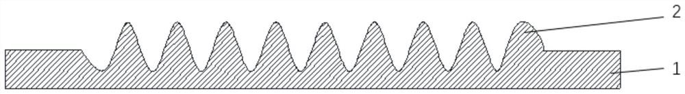
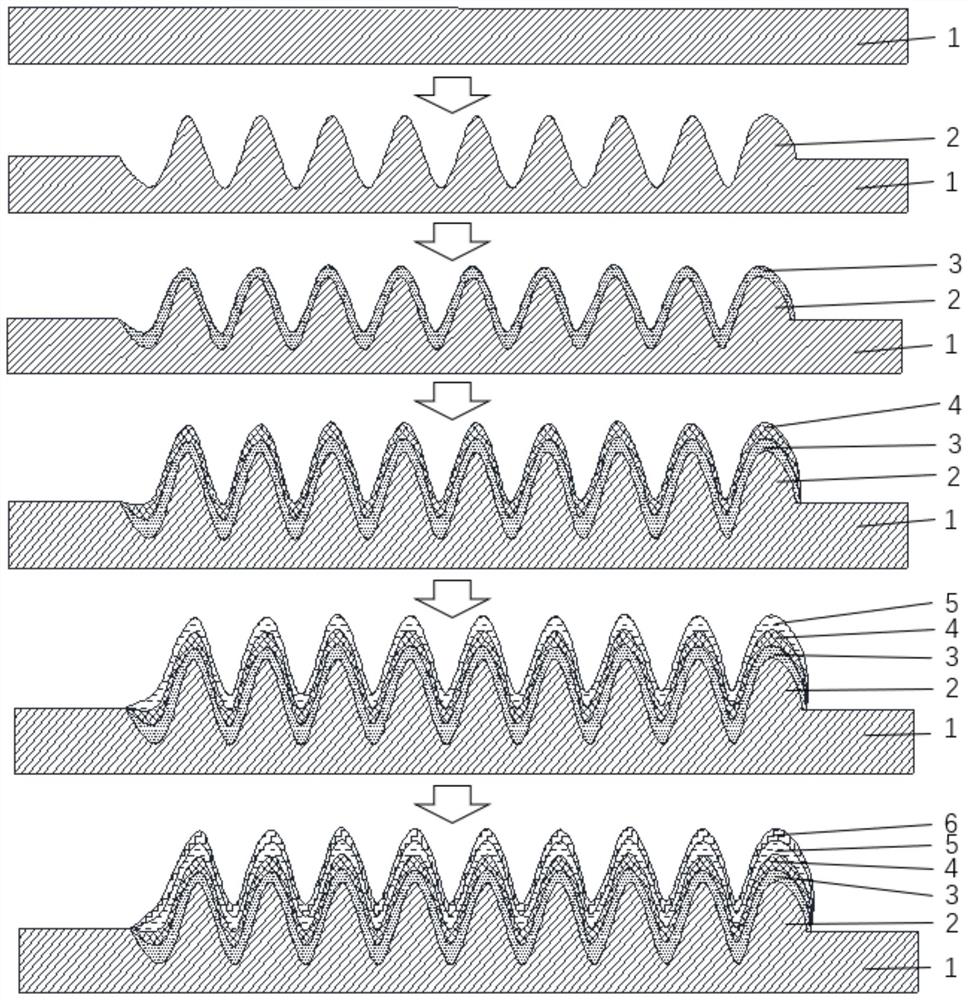
[0042] see image 3 , taking the substrate 1 in a vacuum reaction chamber with a 13.56 MHz plasma radio frequency source, adopting C4F8 and SF6 alternate passivation and etching methods, etching a surface structure with concave-convex lines on one side to form a substrate concave-convex structure 2 The height of the convex part is 6 μm, and the depth of the recess is 5 μm. Of course, besides the etching method in the embodiment, etching methods such as photolithography can also be used, which is not limited by this embodiment.

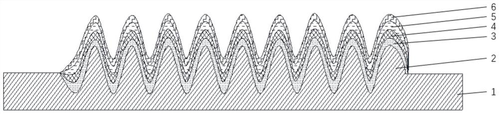
[0043] The vacuum degree is controlled to 1×10⁻⁵ Pa, and the evaporation temperature is 1300 °C, and an aluminum anode 3 with a thickness of 220 nm is prepared on the concave-convex surface of the substrate. The anode 3 is a non-transparent metal, which has high light reflection efficiency and corrosion resistance, improves the light extraction efficiency of the OLED structure, and enhances the brightness of the product.

[0044] Keep the vacuum degre...

Embodiment 2

[0050] see image 3 , taking the substrate in a vacuum reaction chamber with a 13.56 MHz plasma radio frequency source, adopting C4F8 and SF6 alternate passivation and etching methods, etching a surface structure with concave and convex lines on one side to form a substrate concave and convex structure 2, and the height of the convex part is is 1 μm, and the depth of the depressed portion is 10 μm.

[0051] Control the vacuum degree below 1 Pa, use argon and oxygen as the process gas, the specific flow rate of argon gas is 50 sccm, the flow rate of oxygen gas is 0.7 sccm, and magnetron sputtering is used to prepare titanium anode 3 on the concave-convex surface of the substrate with a thickness of 100 nm , the anode 3 is a non-transparent metal, which has high light reflection efficiency and corrosion resistance, and the low light-emitting layer is used to improve the light extraction efficiency of the OLED structure, enhance the brightness of the product and keep the vacuum d...

Embodiment 3

[0056] see image 3 , take the substrate and match it with a 13.56 MHz plasma radio frequency source in a vacuum reaction chamber, etch a surface structure with concave-convex lines on one side to form a substrate concave-convex structure. The height of the convex part is 10 μm, and the depth of the concave part is 1 μm.

[0057] The vacuum degree is controlled to 1×10⁻⁵ Pa, and the evaporation temperature is 1300 °C, and an aluminum anode 3 with a thickness of 220 nm is prepared on the concave-convex surface of the substrate. The anode 3 is a non-transparent metal with high light reflection efficiency and corrosion resistance, and the low light-emitting layer is used to improve the light extraction efficiency of the OLED structure and enhance the brightness of the product.

[0058] Keeping the degree of vacuum below 1×10⁻⁵ Pa, the hole injection layer, the hole transport layer, the light emitting layer, the electron transport layer, and the electron injection layer are sequen...


PUM

PropertyMeasurementUnit
heightaaaaaaaaaa
depthaaaaaaaaaa
thicknessaaaaaaaaaa

Abstract

The invention belongs to the field of display, and provides an OLED structure capable of improving packaging capability, which comprises a substrate, an anode, a composite organic layer, a cathode anda packaging layer stacked in sequence from top to bottom. A substrate concave-convex structure is arranged on one surface of the substrate in contact with the anode, and the concave-convex directionsof the concave-convex structures of the substrates are the same. The OLED device is optimized by taking the substrate configuration as a starting point, and the concave-convex configuration can significantly reduce the surface stress of each film layer and prevent the disassembly and slippage of the film layers, so that the film layers are more stable, the service life of the device is prolonged,and the yield level of the product is improved; meanwhile, due to the concave-convex surface structure, the waveguide mode between organic layers can be reduced, and the plasma mode on the surface ofthe cathode is reduced, so that more light generated in the OLED is emitted, and the light extraction efficiency is improved. The invention further provides a method for preparing the OLED structurecapable of improving the packaging capacity.

Description

technical field [0001] The invention relates to the display field, in particular to an OLED structure and a preparation method thereof. Background technique [0002] Organic light-emitting diodes (OLEDs) have excellent characteristics such as low energy consumption, self-luminescence, and wide viewing angles, and have been widely used in the display industry, such as OLED TVs and tablet computers. With the needs of the economy and society and the advancement of technology, OLED It is more developed towards high definition, curved surface and small size. [0003] In order to meet different requirements for OLED performance, in the prior art, various functional film layers are usually deposited layer by layer on the substrate, but often the surface stress of each film layer is relatively large, and the greater the number of layers, the greater the mutual stress (up to 500 Mpa or more) ), large stress will cause the film to be easily broken and disintegrated. If the bonding fo...

Claims


Application Information

Patent Timeline
Patent Type & Authority Applications(China)
IPC IPC(8): H01L51/52H01L51/56
CPCH10K71/20H10K77/10H10K50/80H10K50/84H10K50/85Y02E10/549
Inventor 王绍华王健波吴远武吴迪
Owner LAKESIDE PHOTOELECTRONICS TECH JIANGSU CO
Why Eureka
Try Eureka