Method for growing bismuth selenide high-index surface single crystal thin film on silicon (211) substrate

A single-crystal thin-film, high-index technology, applied in chemical instruments and methods, crystal growth, single crystal growth, etc., can solve the problems of incompatibility and poor economy, and achieve the effects of good compatibility, simple process and obvious economic benefits

Inactive Publication Date: 2019-06-21
UNIV OF ELECTRONICS SCI & TECH OF CHINA
View PDF5 Cites 4 Cited by
  • Summary
  • Abstract
  • Description
  • Claims
  • Application Information

AI Technical Summary

Problems solved by technology

However, the above-mentioned technologies all use expensive compound semiconductors as Bi 2 Se 3 Substrates for high-index planar thin-film epitaxy, some of which (Document 6) must also use a special buffer layer process, so the economy is poor, and it is not compatible with modern microelectronics processes

Method used


Image

  • Method for growing bismuth selenide high-index surface single crystal thin film on silicon (211) substrate
  • Method for growing bismuth selenide high-index surface single crystal thin film on silicon (211) substrate
  • Method for growing bismuth selenide high-index surface single crystal thin film on silicon (211) substrate

Examples


Embodiment 1

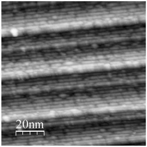
[0041] like figure 1 Shown, the present invention is a kind of method for growing bismuth selenide high-index plane monocrystalline thin film on silicon (211) substrate, comprises the following operation steps:

[0042] Step 1): After placing the Si(211) substrate in an ultra-high vacuum molecular beam epitaxy system, heat it to 500°C for degassing for 12 hours until the background vacuum reaches 5×10 -10 On the order of mbar, continue heating the Si(211) substrate to 1250° C. for 10 seconds, and then lower the temperature to 250° C.

[0043] Step 2): Raise the temperature of the Bi beam source until the equivalent pressure of the Bi beam reaches 3×10 -8 mbar, open the Bi beam source baffle to start growing the Bi buffer layer, the growth time of the Bi buffer layer is 6min, and the growth thickness is

[0044] Step 3): Close the Bi beam source baffle to end the growth of the Bi buffer layer, lower the temperature of the Si(211) substrate to 100°C, and adjust the temperatu...

Embodiment 2

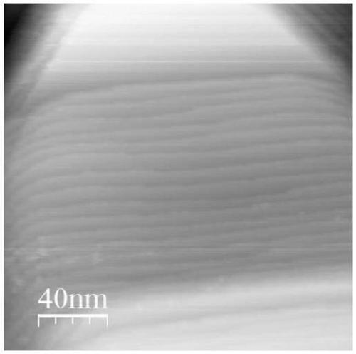
[0051] like figure 1 Shown, the present invention is a kind of method for growing bismuth selenide high-index plane monocrystalline thin film on silicon (211) substrate, comprises the following operation steps:

[0052] Step 1): Before placing the Si(211) substrate in the ultra-high vacuum molecular beam epitaxy system, etch it with 40% HF solution for 2-5 minutes, then rinse it with deionized water and blow it with high-purity nitrogen After drying, the substrate was placed in an ultra-high vacuum molecular beam epitaxy system, heated to 400 ° C for 12 hours, and the background vacuum reached 5 × 10 -10 On the order of mbar, continue heating the Si(211) substrate to 850°C for 10 seconds, and then lower the temperature to 250°C.

[0053] Step 2): Raise the temperature of the Bi beam source until the equivalent pressure of the Bi beam reaches 1×10 -7 mbar, open the Bi beam source baffle to start growing the Bi buffer layer, the growth time of the Bi buffer layer is 2min, and ...


PUM

PropertyMeasurementUnit
thicknessaaaaaaaaaa

Abstract

The invention discloses a method for growing a bismuth selenide high-index surface single crystal thin film on a silicon (211) substrate. The method comprises the following steps: 1), performing flashing silicon treatment or chemical etching treatment on a Si substrate having a crystal plane orientation of (211); 2), raising the temperature of a Bi beam source, depositing and growing a Bi buffer layer on the Si (211) substrate prepared in the step 1); 3), after the Bi buffer layer is grown in the step 2), adjusting the temperature of the Bi beam source, raising the temperature of a Se crackingbeam source, and starting to grow a Bi2Se3 nucleation layer; 4): after the growth of the Bi2Se3 nucleation layer is completed in the step 3, continuing to grow a Bi2Se3 high-index surface single crystal epitaxial thin film to obtain the bismuth selenide high-index surface single crystal thin film. According to the method, the Bi ultra-thin single crystal layer is adopted as a buffer layer, the low-temperature Bi2Se3 nucleation layer with a thickness of 3-5 nm is grown on the surface of the Bi buffer layer, then the growth temperature is appropriately increased to grow the Bi2Se3 high-index surface single crystal thin film epitaxial layer, and the Bi2Se3 high-index surface single crystal thin film having a relatively good crystallinity can be obtained.

Description

technical field [0001] The invention belongs to the field of semiconductor materials, and in particular relates to a method for growing a bismuth selenide high-index plane single crystal thin film on a silicon (211) substrate, in particular, using molecular beam epitaxy equipment on a Si (211) substrate to grow super Growth of Bi by Thin Bi Buffer Layer Method 2 Se 3 (20 45 ) method for orienting high-index planar single-crystal epitaxial films. Background technique [0002] By Bi 2 Se 3 The representative class of traditional thermoelectric materials has been predicted to be a new class of three-dimensional topological insulator materials [Document 1], which has attracted a lot of attention. Topological insulators are a new quantum state of matter, which is completely different from traditional conductors, semiconductors and insulator materials. It is an insulating state with an energy gap in its body, but a metal state without an energy gap on its surface, and has som...

Claims


Application Information

Patent Timeline
Patent Type & Authority Applications(China)
IPC IPC(8): C30B25/18C30B25/16C30B29/46H01L21/02H01L35/16H01L35/34
Inventor 李含冬徐超凡李勇余述鹏尹锡波姬海宁牛晓滨王志明
Owner UNIV OF ELECTRONICS SCI & TECH OF CHINA
Why Eureka
Try Eureka