Amorphous silicon thin film transistor
A technology of transistors and amorphous silicon thin films, applied in the field of thin film transistors, can solve the problem of small signal-to-noise ratio of sensors, and achieve the effects of improving signal-to-noise ratio, reducing noise, and reducing ratio
- Summary
- Abstract
- Description
- Claims
- Application Information
AI Technical Summary
Problems solved by technology
Method used
Image

Examples
preparation example Construction
[0052] The present invention also provides a method for preparing the above-mentioned thin film transistor, comprising the following steps:
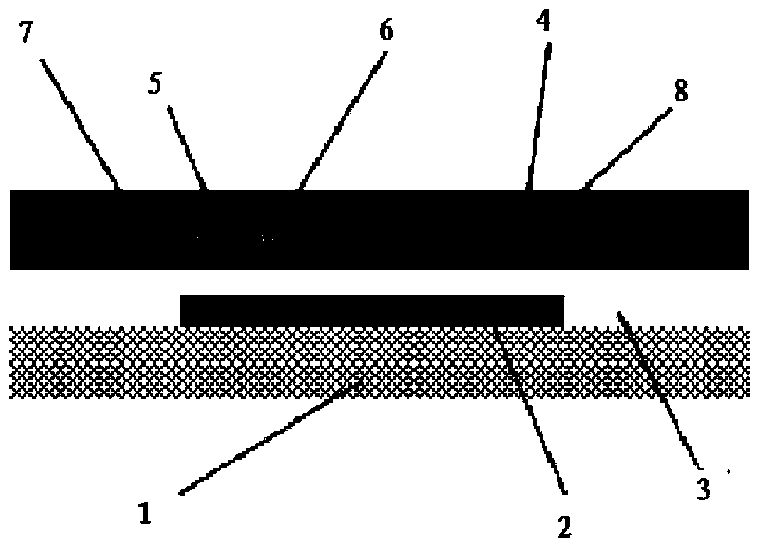
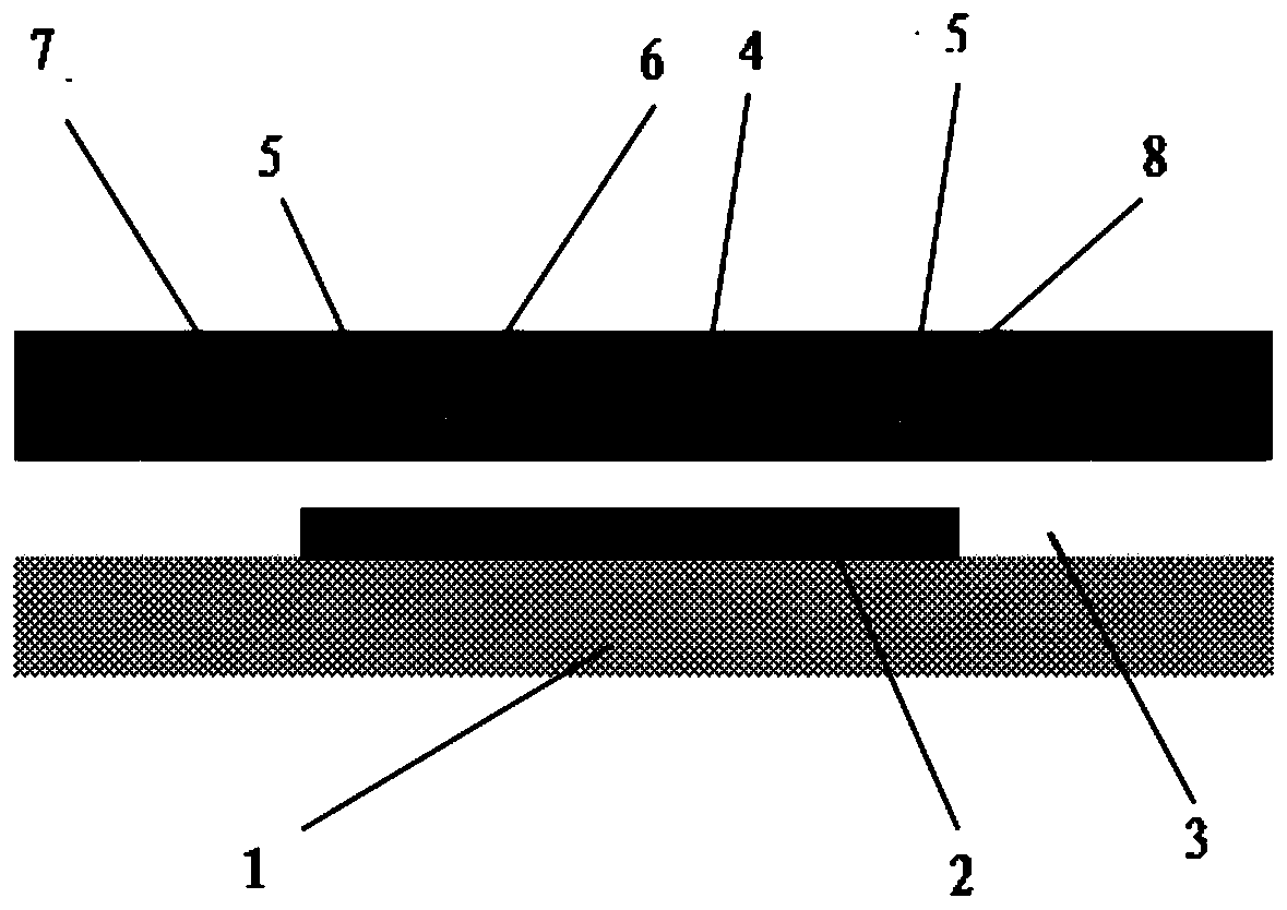
[0053] Forming a substrate 1, a gate 2, a gate insulating layer 3 and an amorphous silicon semiconductor layer 4 sequentially on the surface of the substrate along the direction extending toward the inner surface of the substrate;
[0054] Conduction band energy layers 5 are respectively formed on one or both end surfaces of the amorphous silicon semiconductor layer, and;
[0055]Ohmic contact layers 7 are respectively formed on the conduction band energy layer 5 combined with the two ends of the amorphous silicon semiconductor layer 4; or on the conduction band distributed at one end of the amorphous silicon semiconductor layer 4 An ohmic contact layer 7 is formed on the energy layer 5, and the ohmic contact layer 7 is directly formed on the other end of the amorphous silicon semiconductor layer 4;
[0056] A source electrode and a dra...
Embodiment 1
[0064] The amorphous silicon thin film transistor of one embodiment of the present invention is as figure 1 Shown includes: a glass substrate 1; a gate 2, bonded to one surface of the substrate 1; a gate insulating layer 3, bonded to the surface of the substrate, and covering the gate 2; a semiconductor layer, bonded to the gate insulating layer on the surface away from the substrate; the semiconductor layer includes an amorphous silicon semiconductor layer 4; the amorphous silicon semiconductor layer 4 is combined on the surface of the gate insulating layer 3 away from the gate 2; the ohmic contact layer 7 includes each other The two parts of the interval are respectively combined on both ends of the surface of the amorphous silicon semiconductor layer away from the gate insulating layer; the source electrode and the drain electrode are respectively combined on the ohmic contact layer 7 ; and the passivation layer 8 . The semiconductor layer also includes a conduction band en...
Embodiment 2
[0072] The amorphous silicon thin film transistor of one embodiment of the present invention is as figure 1 Shown includes: a glass substrate 1; a gate 2, bonded to one surface of the substrate 1; a gate insulating layer 3, bonded to the surface of the substrate, and covering the gate 2; a semiconductor layer, bonded to the gate insulating layer on the surface away from the substrate; the semiconductor layer includes an amorphous silicon semiconductor layer 4; the amorphous silicon semiconductor layer 4 is combined on the surface of the gate insulating layer 3 away from the gate 2; the ohmic contact layer 7 includes each other The two parts of the interval are respectively combined on both ends of the surface of the amorphous silicon semiconductor layer away from the gate insulating layer; the source electrode and the drain electrode are respectively combined on the ohmic contact layer 7 ; and the passivation layer 8 . The semiconductor layer also includes a conduction band en...
PUM
 Abstract
Description
Claims
Application Information
 - Generate Ideas
- Intellectual Property
- Life Sciences
- Materials
- Tech Scout
- Unparalleled Data Quality
- Higher Quality Content
- 60% Fewer Hallucinations
Browse by: Latest US Patents, China's latest patents, Technical Efficacy Thesaurus, Application Domain, Technology Topic, Popular Technical Reports.
© 2025 PatSnap. All rights reserved.Legal|Privacy policy|Modern Slavery Act Transparency Statement|Sitemap|About US| Contact US: help@patsnap.com