Method for preparing a-Si: H thin film based on hydrogen plasma treatment

A plasma, a-si technology, used in semiconductor devices, final product manufacturing, sustainable manufacturing/processing, etc., can solve problems such as affecting passivation effect, epitaxial growth, reducing silane decomposition rate, etc., to improve passivation quality Effect

Inactive Publication Date: 2019-06-28
上海米蜂激光科技有限公司
View PDF6 Cites 3 Cited by
  • Summary
  • Abstract
  • Description
  • Claims
  • Application Information

AI Technical Summary

Problems solved by technology

Higher hydrogen dilution may lead to epitaxial growth at the amorphous silicon / crystalline silicon interface, affecting the passivation effect; lower RF power density, on the one hand, will reduce the decomposition rate of silane, on the other hand, with the amorphous silicon With the prolongation of silicon film deposition time, more and more low-order silicon hydrogen elements such as SiH2 and SiH will also be produced, which will affect the quality of amorphous silicon film

Method used


Image

  • Method for preparing a-Si: H thin film based on hydrogen plasma treatment
  • Method for preparing a-Si: H thin film based on hydrogen plasma treatment
  • Method for preparing a-Si: H thin film based on hydrogen plasma treatment

Examples


Embodiment 1

[0023] First, the substrate is cleaned. A 250um thick (100) oriented phosphorus-doped N-type double-polished CZ silicon wafer (resistivity 5-10Ωcm) was used as the substrate, and a simplified RCA method was used before the deposition of the amorphous silicon film (Wang Nan, Zhang Yu, Zhou Yuqin. Research on the key process of interface treatment of silicon heterojunction cells [J]. Journal of Synthetic Crystals, 2013, 42(2): 000235-239.) Removal of organic contamination and metal impurities on the surface of silicon wafers.

[0024] Then, the chemical pretreatment of the substrate is carried out. The silicon wafer cleaned by the simplified RCA method was immersed in a dilute HF solution (concentration: 3%), and then the silicon wafer was placed in a deionized water (80°C) water bath for 60 minutes; before a-Si:H thin film deposition, the The cleaned silicon wafer was immersed in dilute HF solution (concentration: 3%) again and blown dry with nitrogen gas.

[0025] Table 1. D...

Embodiment 2

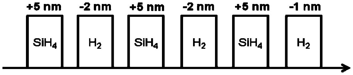
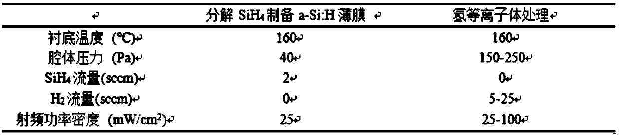
[0031] On the one hand, the hydrogen plasma treatment process can interrupt the deposition process of a-Si:H film to avoid the generation of low-order silicon-hydrogen units, and on the other hand, it can also inject the atomic hydrogen produced by decomposition into the a-Si:H film. Fill the electrical defects in the a-Si:H film and the dangling bond states on the saturated c-Si surface to improve the passivation effect of the a-Si:H / c-Si interface.

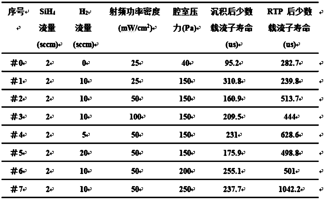
[0032] Table 2. Embodiment 2 experimental data

[0033]

[0034] See Table 2, where the samples numbered #0 are a-Si:H film deposition for the decomposition of pure SiH4, and the samples numbered #1-#7 are a-Si prepared by periodically interrupting the decomposition of pure SiH4 by hydrogen plasma : Deposition process of H film and hydrogen plasma treatment of the film. Microwave photoconductivity decay method was used to measure the minority carrier lifetime of thin film samples after deposition and rapid thermal annealing ...


PUM

PropertyMeasurementUnit
Resistivityaaaaaaaaaa

Abstract

The invention relates to the technical field of preparation methods of a-Si: H, in particular to a method for preparing an a-Si: H thin film based on hydrogen plasma treatment. The method includes steps that a, SiH4 is decomposed in a depositing cavity to deposit the a-Si: H thin film; and b, depositing stops, remaining gas in the depositing cavity is discharged, then H2 is introduced into the depositing cavity, and is decomposed to form hydrogen plasma which acts on an amorphous silicon thin film, and the step a and the step b are alternately adopted to finally obtain the a-Si: H thin film ata set thickness. The method has the beneficial effects that compared with the prior art, according to the periodically alternated hydrogen plasma treatment process adopted by the method, by interrupting production of low-order silicon and hydrogen elements or etching the a-Si: H thin film high in content of the low-order silicon and hydrogen elements, the passivating quality is remarkably improved; and more atomic hydrogen is injected into the a-Si: H thin film, in cooperation with the later period high temperature fast heat treatment process, a basis is laid for filling up the electrical defects in the a-Si: H thin film and saturating the dangling bond state of the c-Si surface, and therefore the passivating quality is remarkably improved.

Description

technical field [0001] The present invention relates to the technical field of preparation methods of a-Si:H, in particular to a method for preparing a-Si:H thin films based on hydrogen plasma treatment. Background technique [0002] Recently, the highest laboratory efficiency of 25.6% has been achieved for silicon heterojunction solar cells. Compared with the traditional monocrystalline silicon cell, this type of cell uses a wide bandgap intrinsic amorphous silicon thin layer (5nm~10nm) as the emission layer, so that the open circuit voltage is very high (~740mv), and the thin layer acts as a passivation layer. The layer is used to saturate the dangling bonds on the surface of crystalline silicon and reduce the generation of leakage current. Therefore, it is necessary to prepare "device-grade" amorphous silicon thin films with low electrical defect density and good microstructural properties to improve cell efficiency. In industry, the RF-PECVD system is usually used to d...

Claims


Application Information

Patent Timeline
IPC IPC(8): C23C16/02C23C16/24C23C16/513H01L31/20
CPCY02P70/50
Inventor 王楠钟奇谢雨江
Owner 上海米蜂激光科技有限公司
Why Eureka
Try Eureka