Preparation method of stackable large-area nano wire intersected lattice array resistive switching memory device structure

A technology of silicon nanowire array and resistive variable storage, which is applied in the direction of electrical components and can solve the problems of large-scale integration of memristive units

Active Publication Date: 2019-06-28
NANJING UNIV
View PDF8 Cites 6 Cited by
  • Summary
  • Abstract
  • Description
  • Claims
  • Application Information

AI Technical Summary

Problems solved by technology

Compared with traditional oxide memristors, two-dimensional material memristors can withstand harsh environments such as high temperature and pressure, and can meet the heat resistance requirements of electronic components in aerospace, military, oil and gas exploration and other applications. But large-scale integration of memristive cells has become a big problem

Method used


Image

  • Preparation method of stackable large-area nano wire intersected lattice array resistive switching memory device structure
  • Preparation method of stackable large-area nano wire intersected lattice array resistive switching memory device structure
  • Preparation method of stackable large-area nano wire intersected lattice array resistive switching memory device structure

Examples


Embodiment Construction

[0031] The present invention will be further described below in conjunction with the accompanying drawings and embodiments.

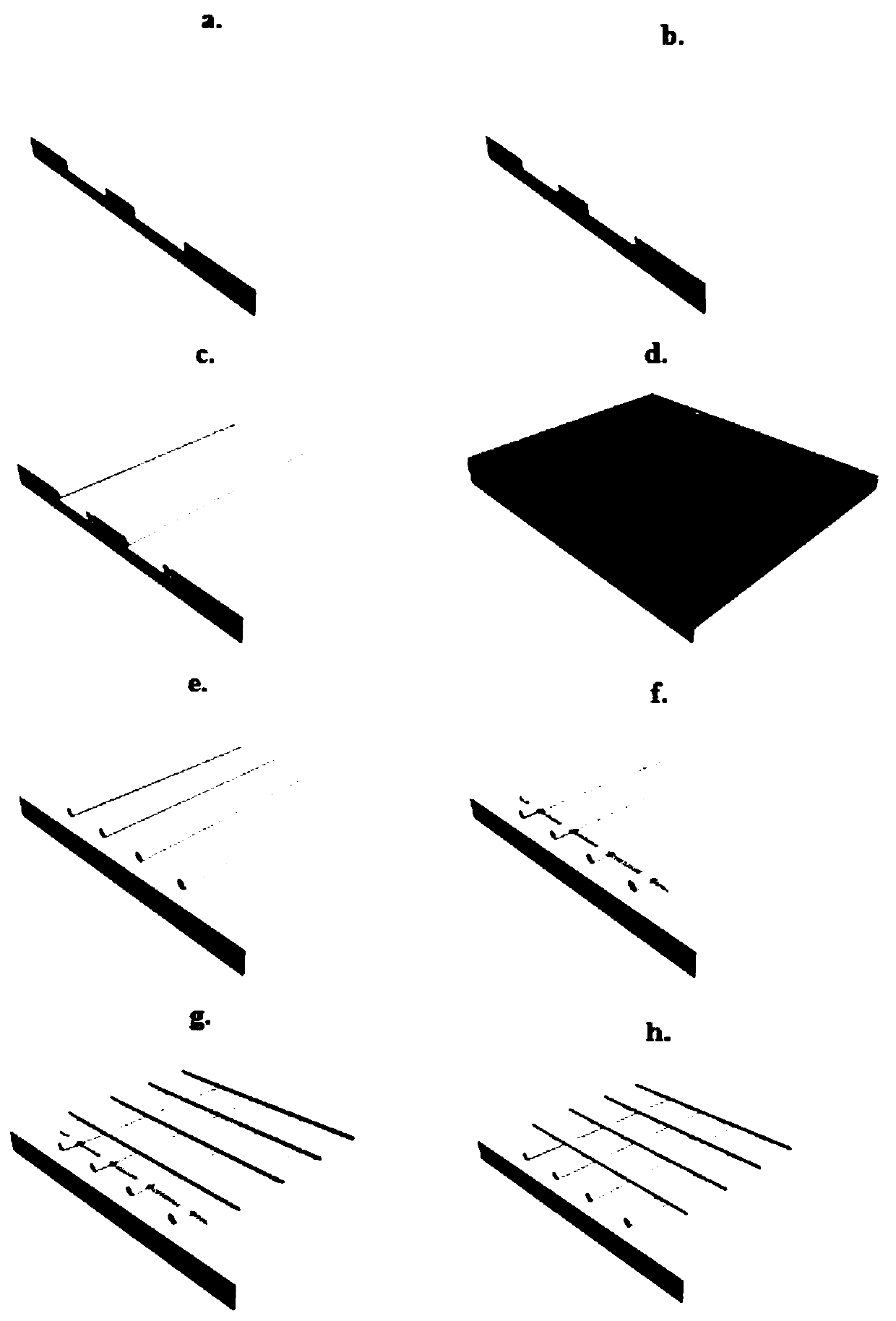
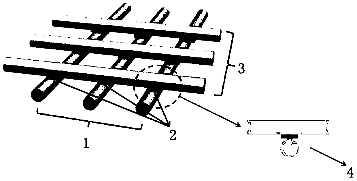
[0032] Such as figure 1 Shown is a method for fabricating a nanowire intersection array resistive memory device structure that can be stacked and prepared in a large area, which specifically includes the following steps:

[0033] 1) Process the pure silicon wafer in PECVD equipment to obtain a silicon oxide wafer covered with a silicon dioxide layer, that is, a silicon-based substrate;

[0034] 2) Define the growth guide channel on the surface of the silicon oxide wafer by means of photolithography, electron beam direct writing (EBL) or mask, and use inductively coupled plasma (ICP) etching or reactive plasma etching (RIE), etc. Technology Dry etching of exposed silicon-based substrates, in which reactive gases with different chemical properties such as SF6, CF4 (or their mixed gases) can be used as etchant to form planar distribution etching channels;...


PUM

PropertyMeasurementUnit
Thicknessaaaaaaaaaa
Diameteraaaaaaaaaa
Thicknessaaaaaaaaaa

Abstract

The invention discloses a preparation method of a stackable large-area nano wire intersected lattice array resistive switching memory device structure. The preparation method comprises that a resin colloid material transfer method is used to realize alternative stacking and intersected distribution of a silicon nano wire array and a film material, and a film interlayer silicon nano wire intersected lattice array structure of the 3D space is formed; and in the alternative stacking process, the top silicon nano wire serves as a mask, an etching device is used to etch the film material not shielded by nano wires in the grid part, an extremely low point contact structure of a nano wire intersection point and interlayer film material is obtained, and a vertical conductive channel of extremely high alignment is provided for the memory device. According to the method, it is not required to introduce the high-cost micronano control technology (as a nano mechanical arm), only a simple transfertechnology is used to realize directed stacking of the nano material, the silicon nano wire serves as the master to realize accurate etching of the film material, and the electronic device of the nano-level sandwich type point-to-point contact structure is prepared reliably.

Description

technical field [0001] The invention relates to a method for preparing a nanowire intersection array resistive memory device structure that can be stacked and prepared in a large area, and belongs to the field of semiconductor micro-nano electronic devices, especially for large-area memristive devices, 3D logic, flexible / wearable electronics and Field-effect biochemical sensing devices. Background technique [0002] Bulk silicon material is an important traditional semiconductor material, which is the raw material for manufacturing semiconductor silicon devices, and is used to make high-power rectifiers, high-power transistors, diodes, switching devices, etc. Its follow-up products, integrated circuits and semiconductor separation devices, have been widely used in various fields, and also occupy an important position in military electronic equipment. As an important class of one-dimensional semiconductor nanomaterials, silicon nanowires (nanowires), which are developed from...

Claims


Application Information

Patent Timeline
IPC IPC(8): H01L45/00
Inventor 余林蔚刘川吴琦王军转
Owner NANJING UNIV
Why Eureka
Try Eureka