Flexible color micro-LED manufacturing method and prepared product

A flexible and color technology, applied in the direction of instruments, electrical components, electric solid devices, etc., can solve the problems of huge amount of chips, color conversion, transfer, etc. Effect

Active Publication Date: 2019-07-02
SHANTOU UNIV
View PDF7 Cites 3 Cited by
  • Summary
  • Abstract
  • Description
  • Claims
  • Application Information

AI Technical Summary

Problems solved by technology

However, its industrialization still faces many problems such as: miniaturization and arrayization, transfer of a large number of chips, color transformation, detection and repair, etc.

Method used


Image

  • Flexible color micro-LED manufacturing method and prepared product
  • Flexible color micro-LED manufacturing method and prepared product
  • Flexible color micro-LED manufacturing method and prepared product

Examples


Embodiment 1

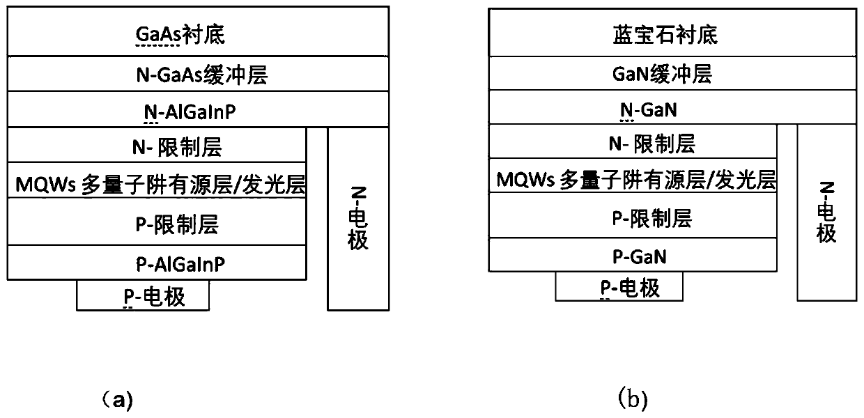
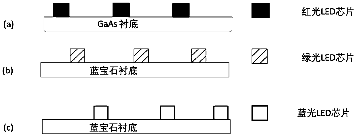
[0024] Step 1. Prefabricate a patterned red light flip-chip microchip (pixel) on the GaAs substrate LED wafer (including epitaxial layer) by photoetching or mutual induction coupled plasma etching (ICP) (see attached figure 1 (a), with a size of 8 μm. The fabricated Micro-LED chip is annealed in a vacuum furnace.

[0025] Step 2. Make patterned GaN-based green and blue flip-chips (pixels) on the sapphire substrate LED wafer (including epitaxial layer) by photoetching or inductively coupled plasma etching (ICP) respectively (see attached figure 1 (b) and (c)), with a size of 8 μm. The green and blue chips produced were annealed in a vacuum furnace respectively.

[0026] Step 3, performing selective etching on the GaAs substrate of the red light microchip to obtain a patterned chip supported by a thin film.

[0027] Step 4, the sapphire substrates on the green light and blue light microchips are respectively peeled off by laser.

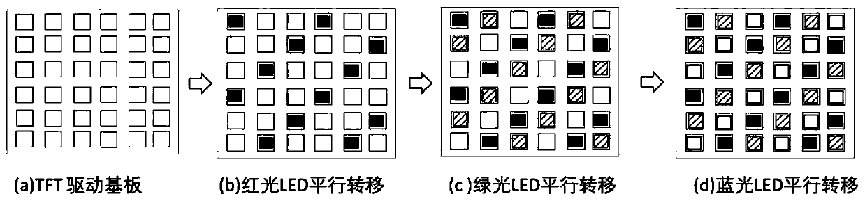
[0028] Step 5. Translate the pattern-shaped ...

Embodiment 2

[0034] Step 1. Prefabricate a patterned red light flip-chip microchip (pixel) on the GaAs substrate LED wafer (including epitaxial layer) by photoetching or mutual induction coupled plasma etching (ICP) (see attached figure 1 (a), with a size of 7 µm. The fabricated Micro-LED chip is annealed in a vacuum furnace.

[0035] Step 2. Make patterned GaN-based green and blue flip-chips (pixels) on the sapphire substrate LED wafer (including epitaxial layer) by photoetching or inductively coupled plasma etching (ICP) respectively (see attached figure 1 (b) and (c)), with a size of 7 microns. The green and blue chips produced were annealed in a vacuum furnace respectively.

[0036] Step 3, performing selective etching on the GaAs substrate of the red light microchip to obtain a patterned chip supported by a thin film.

[0037] Step 4, the sapphire substrates on the green light and blue light microchips are respectively peeled off by laser.

[0038] Step 5. Translate the pattern-sh...

Embodiment 3

[0044] Step 1. Prefabricate a patterned red light flip-chip microchip (pixel) on the GaAs substrate LED wafer (including epitaxial layer) by photoetching or mutual induction coupled plasma etching (ICP) (see attached figure 1 (a), with a size of 6 μm. The fabricated Micro-LED chip is annealed in a vacuum furnace.

[0045]Step 2. Make patterned GaN-based green and blue flip-chips (pixels) on the sapphire substrate LED wafer (including epitaxial layer) by photoetching or inductively coupled plasma etching (ICP) respectively (see attached figure 1 (b) and (c)), with a size of 6 microns. The green and blue chips produced were annealed in a vacuum furnace respectively.

[0046] Step 3, performing selective etching on the GaAs substrate of the red light microchip to obtain a patterned chip supported by a thin film.

[0047] Step 4, the sapphire substrates on the green light and blue light microchips are respectively peeled off by laser.

[0048] Step 5. Translate the pattern-sha...


PUM

PropertyMeasurementUnit
sizeaaaaaaaaaa

Abstract

The embodiment of the invention discloses a flexible color micro-LED manufacturing method and a prepared product. The method comprises steps of: (1) preparing a red-light miniaturized patterned flip-chip based on a GaAs substrate; (2) preparing sapphire-based green-light and blue-light miniaturized patterned flip-chips; (3) annealing the chips to improve external quantum efficiency; (4) selectively etching the GaAs substrate and laser stripping off the sapphire substrate; (5) transferring the green-light, blue-light, and red-light film chips to a driving substrate in batches at a time, and separating the respective chips by ICP etching; (6) soldering the chips to the driving substrate; (7) removing Si and silicon oxide buffer layers by mechanical polishing and chemical etching to strip offthe Si substrate; and (8) transferring the chips and integrating the chips into the poly-dimethyl siloxane by using a rubber stamp transfer method. The method has a large transfer amount, is simple,convenient and fast, reduces the number and time of transfer, and can directly obtain RGB three primary colors and perform intrinsic color conversion, thereby greatly improving the display quality andreducing the production cost of the Micro-LED.

Description

technical field [0001] The invention relates to the technical field of semiconductors and flexible electronics, in particular to a method for preparing a flexible color Micro-LED and a prepared product. Background technique [0002] Compared with the existing OLED technology, Micro-LED, a new generation of display technology, not only has the characteristics of high luminous efficiency, high brightness and lower power consumption, but also is not easily affected by water vapor, oxygen or high temperature, so its stability, service life , working temperature and other aspects have obvious advantages. Compared with the image response speed of TFT-LCD in milliseconds and the microseconds of OLED, the image response speed of Micro-LED is only nanoseconds. Secondly, the display screen as a wearable electronic device accounts for 80% of the power consumption; Micro-LED The characteristics of low power consumption and fast response speed are most suitable for VR / AR equipment, vehi...

Claims


Application Information

Patent Timeline
Patent Type & Authority Applications(China)
IPC IPC(8): H01L27/15G09F9/30
CPCG09F9/301H01L27/156
Inventor 徐从康顾而丹王江涌
Owner SHANTOU UNIV
Why Eureka
Try Eureka