Phase change material, phase change storage unit and preparation method thereof

A technology of phase change material and phase change memory, which is applied in the field of microelectronics, can solve the problems that the speed requirement of DRAM cannot be met, the data retention cannot be guaranteed, and the phase change speed of data loss is outstanding, achieving outstanding thermal stability, The effect of high yield and fast phase change

Active Publication Date: 2019-07-26
SHANGHAI INST OF MICROSYSTEM & INFORMATION TECH CHINESE ACAD OF SCI
View PDF12 Cites 12 Cited by
  • Summary
  • Abstract
  • Description
  • Claims
  • Application Information

AI Technical Summary

Problems solved by technology

[0006] In view of the shortcomings of the prior art described above, the purpose of the present invention is to provide a phase change material, a phase change memory unit and a preparation method thereof, which are used to solve the problem of low crystallization temperature and thermal stability of the phase change material in the prior art. The performance is not good, the data retention cannot be guaranteed, and it faces the problem of data loss and the low phase change speed, which cannot meet the speed requirements of DRAM.

Method used


Image

  • Phase change material, phase change storage unit and preparation method thereof
  • Phase change material, phase change storage unit and preparation method thereof
  • Phase change material, phase change storage unit and preparation method thereof

Examples


Embodiment 1

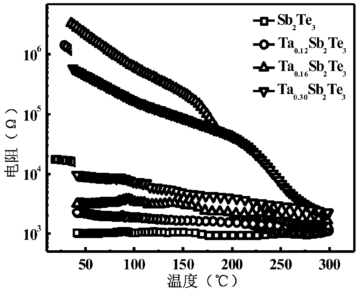
[0031] A phase change material is provided in this embodiment, the phase change material includes tantalum (Ta) element, antimony (Sb) element and tellurium (Te) element, and the chemical formula of the phase change material is Ta x Sb y Te z , wherein, x, y, z all refer to the atomic percentage of elements, and 1≤x≤25, 0.5≤y:z≤3, x+y+z=100.

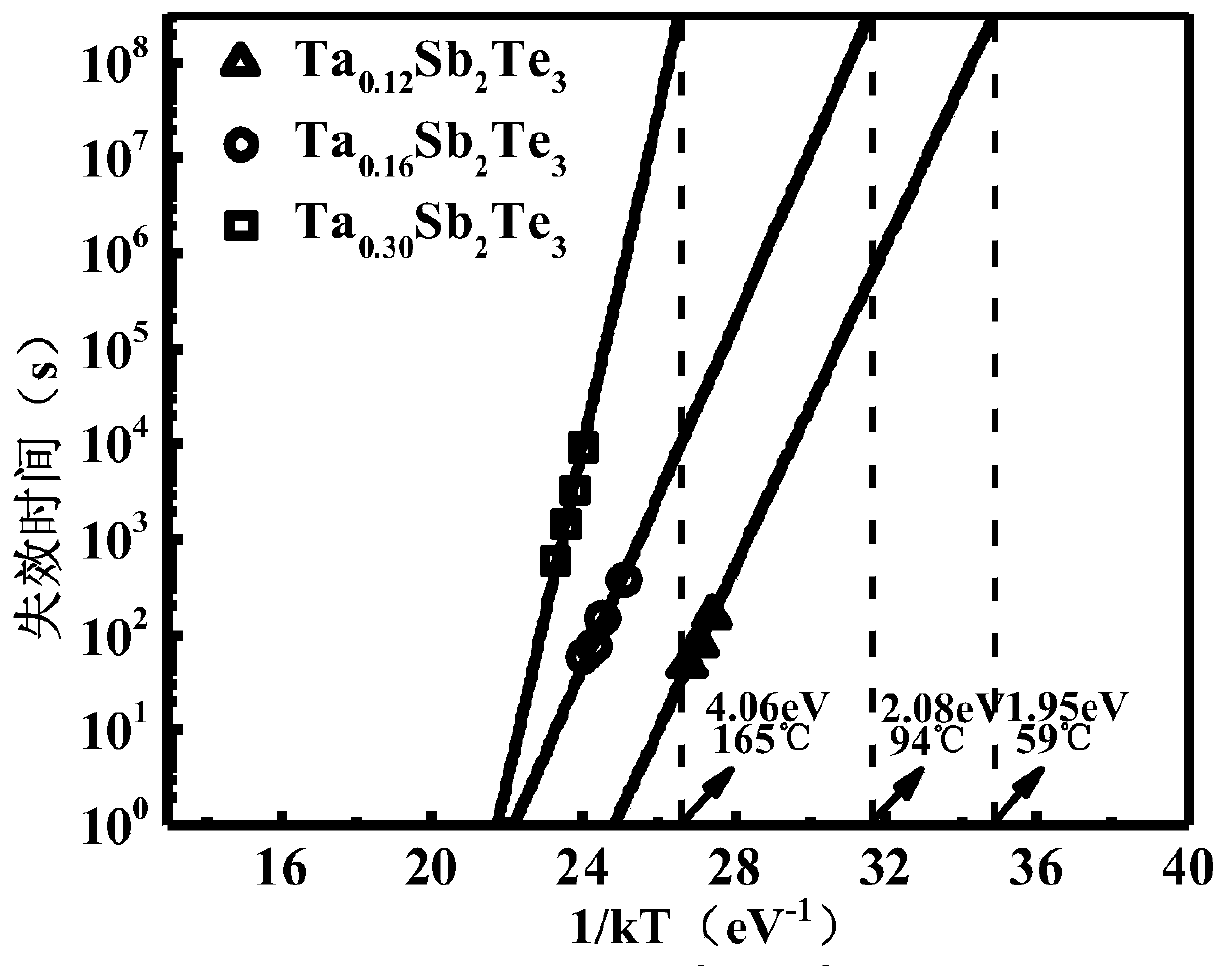
[0032] Specifically, the Ta x Sb y Te z In , the contents of the three elements can be adjusted to obtain storage materials with different crystallization temperatures, resistivities, and crystallization activation energies. For example, the Ta x Sb y Te zAmong them, it can further satisfy 2≤x≤10, 25≤y≤45, 40≤z≤70, or further satisfy 3.5≤x≤9, 30≤y≤40, 50≤z≤60, and further satisfy 4≤ x≤8, 36≤y≤39.6, 54≤z≤59.4. In this embodiment, x, y, and z preferably satisfy: x=5.7, y=37.7, z=56.6, that is, the chemical formula of the phase change material is Ta 5.7 Sb 37.7 Te 56.6 .

[0033] Specifically, the Ta x Sb y Te z The phase-ch...

Embodiment 2

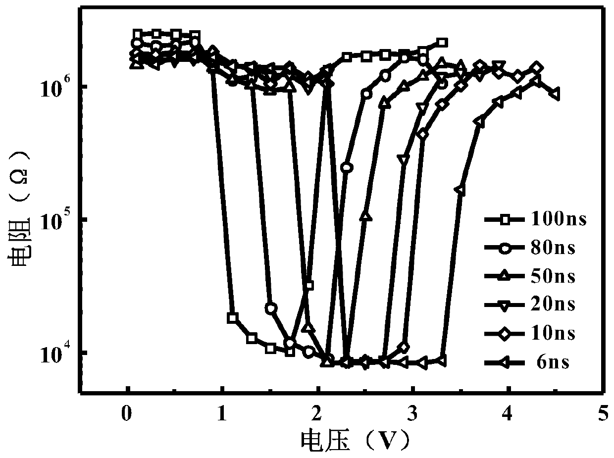
[0041] In this embodiment, a phase-change memory unit is provided, and the phase-change memory unit includes a lower electrode layer, an upper electrode layer, and a phase-change material layer between the lower electrode layer and the upper electrode layer. The variable material layer comprises Ta as described in Example 1 x Sb y Te z Phase change material, that is, the phase change material includes tantalum (Ta) element, antimony (Sb) element and tellurium (Te) element, and the chemical formula of the phase change material is Ta x Sb y Te z , wherein, x, y, z all refer to the atomic percentage of elements, and 1≤x≤25, 0.5≤y:z≤3, x+y+z=100.

[0042] As an example, the thickness range of the phase change material layer is 20nm-150nm.

[0043] As an example, an extraction electrode is formed on the upper electrode layer, through which the upper electrode layer and the lower electrode layer can be integrated with control switches, driving circuits and peripheral circuits o...

Embodiment 3

[0048] In this embodiment, a method for preparing a phase-change memory cell is provided, including the following steps:

[0049] S1: preparing the lower electrode layer;

[0050] S2: Prepare a phase-change material layer on the lower electrode layer, the phase-change material layer includes the phase-change material described in Example 1, that is, the phase-change material includes tantalum (Ta) elements, antimony (Sb) element and tellurium (Te) element, the chemical formula of the phase change material is Ta x Sb y Te z , wherein, x, y, z all refer to the atomic percentage of elements, and 1≤x≤25, 0.5≤y:z≤3, x+y+z=100. ;

[0051] S3: preparing an upper electrode layer on the phase change material layer.

[0052] As an example, the lower electrode layer may be prepared by a sputtering method, an evaporation method, a chemical vapor deposition (CVD), a plasma enhanced chemical vapor deposition (PECVD), or the like. The material of the lower electrode layer includes: one...


PUM

PropertyMeasurementUnit
particle sizeaaaaaaaaaa
thicknessaaaaaaaaaa
thicknessaaaaaaaaaa

Abstract

The invention provides a phase change material, a phase change storage unit and a preparation method thereof, wherein the phase change material comprises a tantalum element, an antimony element and atellurium element, wherein the chemical formula of the phase change material is TaxSbyTez, wherein x, y and z refer to atomic percentages of elements, wherein x is greater than or equal to 1 and lessthan or equal to 25, y is greater than or equal to 0.5, z is less than or equal to 3, and x+y+z is equal to 100. The TaxSbyTez phase change film material disclosed by the invention has the characteristics of being high in phase change speed, outstanding in heat stability, high in data retention capability, long in cycle life, high in rate of finished products and the like, wherein Ta5.7Sb37.7Te56.6 has 10 years of data retention at 165 DEG C, and when being applied to a phase change storage device unit, the operation speed of 6ns and the erase number of one million or above can be achieved; meanwhile, the TaxSbyTez phase change material has very small crystal particles, and the sizes of the crystal particles is still smaller than 30 nm after annealing treatment at 400 DEG C for 30min, which is very important for stability, low power consumption and finished product rate of the device. The preparation method of the phase change memory unit is compatible with a CMOS process and is convenient for accurately controlling the components of the phase change material.

Description

technical field [0001] The invention belongs to the technical field of microelectronics, and relates to a phase-change material, a phase-change storage unit and a preparation method thereof. Background technique [0002] Phase-change memory (PCM) is a non-volatile semiconductor memory that has developed rapidly in recent years. Compared with traditional memory, it has the advantages of non-volatility, good miniaturization, fast read and write speed, low power consumption, long cycle life and excellent radiation resistance. Therefore, phase change memory has become the most powerful competitor in various new storage technologies, and is expected to become the mainstream storage technology of the next generation of non-volatile memory. At present, because its performance such as speed and cycle life is between flash memory (FLASH) and dynamic random access memory (DRAM), it is expected to be applied in new fields, such as storage class memory (Storage Class Memory). [0003]...

Claims


Application Information

Patent Timeline
Patent Type & Authority Applications(China)
IPC IPC(8): H01L45/00
CPCH10N70/021H10N70/8828H10N70/231H10N70/026H10N70/826H10N70/023
Inventor 宋三年薛媛宋志棠
Owner SHANGHAI INST OF MICROSYSTEM & INFORMATION TECH CHINESE ACAD OF SCI
Why Eureka
Try Eureka