

High-purity silicon carbide, silicon carbide wafer and preparation method of high-purity silicon carbide
A technology of high-purity silicon carbide and silica, which is applied in the direction of silicon carbide, chemical instruments and methods, carbide, etc., can solve the problems of high cost and complicated manufacturing process of high-purity silicon carbide, and achieve good crystal integrity and uniform resistivity , the effect of uniform crystal form
- Summary
- Abstract
- Description
- Claims
- Application Information
AI Technical Summary
Problems solved by technology
Method used
Image

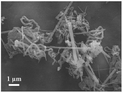
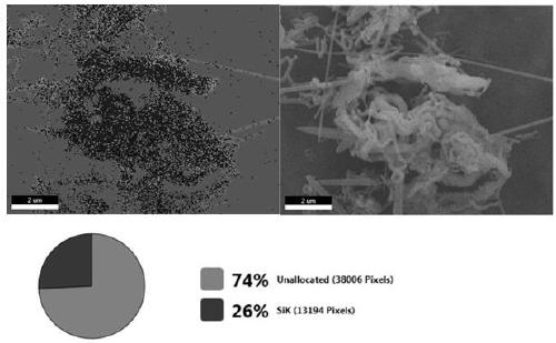
Examples
Embodiment 1
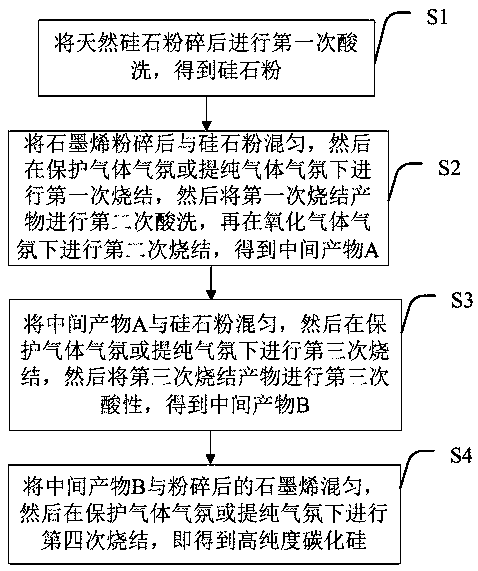
[0054] (1) The natural silica is crushed to a particle size of about 5 μm by a double-roller mill, and transferred to HNO with a concentration of 1 mol / L 3 and 3 mol / L of H 2 SO 4 After immersing in the mixed solution for 50 min, filter it, rinse the solid material with deionized water, and dry it in a vacuum oven at 150°C.
[0055] (2) Weigh 100.0 g of treated silica powder and 10.0 g of pulverized graphene powder, place them in a 500 ml polytetrafluoroethylene tank, add 200.0 g of agate beads, and ball mill for 18 hours to obtain a solid mixture; The solid mixture was placed in a high-temperature carbonization furnace with argon as a protective gas, and calcined at 1900 °C for 13 h to obtain a pre-treated sample; the pre-treated sample was soaked in 5 mlol / L HF solution, mixed and stirred for 50 min, and passed through a bag type After filtering, it was transferred to a muffle furnace and calcined at 420 °C for 4 h under an air atmosphere to obtain intermediate product A. ...
Embodiment 2
[0062] (1) The natural silica is crushed to a particle size of about 5 μm by a double-roller mill, and transferred to HNO with a concentration of 1 mol / L 3 and 2 mol / L of H 2 SO 4 After immersing in the mixed solution for 50 min, filter it, rinse the solid material with deionized water, and dry it in a vacuum oven at 150°C.
[0063](2) Weigh 60.0 g of treated silica powder and 10.0 g of pulverized graphene powder, put them in a 500 ml polytetrafluoroethylene tank, add 200.0 g of agate beads, and ball mill for 11 h to obtain a solid mixture. The solid mixture was placed in a high-temperature carbonization furnace with argon as a protective gas, and calcined at 1350 °C for 13 h to obtain a pre-treated sample, which was soaked in 2 mlol / L HF solution, mixed and stirred for 40 min, and passed through a bag type After filtering, it was transferred to a muffle furnace and calcined at 650 °C for 4 h under an air atmosphere to obtain intermediate product A.
[0064] (3) Weigh 560.0...
PUM
| Property | Measurement | Unit |
|---|---|---|
| particle size | aaaaa | aaaaa |
| particle diameter | aaaaa | aaaaa |
| diameter | aaaaa | aaaaa |
Abstract
Description
Claims
Application Information