A method for forming an air gap

An air-gap and sheet-like technology, applied in the field of air-gap, can solve the problems of increased effective dielectric constant, complicated process, and narrowed grooves, and achieve the effects of improving product performance, simplifying the integration process, and increasing the forming ratio

Active Publication Date: 2021-08-31
SHANGHAI INTEGRATED CIRCUIT RES & DEV CENT +1
View PDF3 Cites 0 Cited by
  • Summary
  • Abstract
  • Description
  • Claims
  • Application Information

AI Technical Summary

Problems solved by technology

[0004] (1) The process is complex and requires additional processes such as patterning and planarization;
[0005] (2) Non-conformal CVD film formation technology will still have a large number of thin films deposited in the air gap, resulting in the actual mention of the air gap being smaller than that of the groove between interconnect lines, and the effective dielectric constant is increased.

Method used


Image

  • A method for forming an air gap
  • A method for forming an air gap
  • A method for forming an air gap

Examples


Embodiment 1

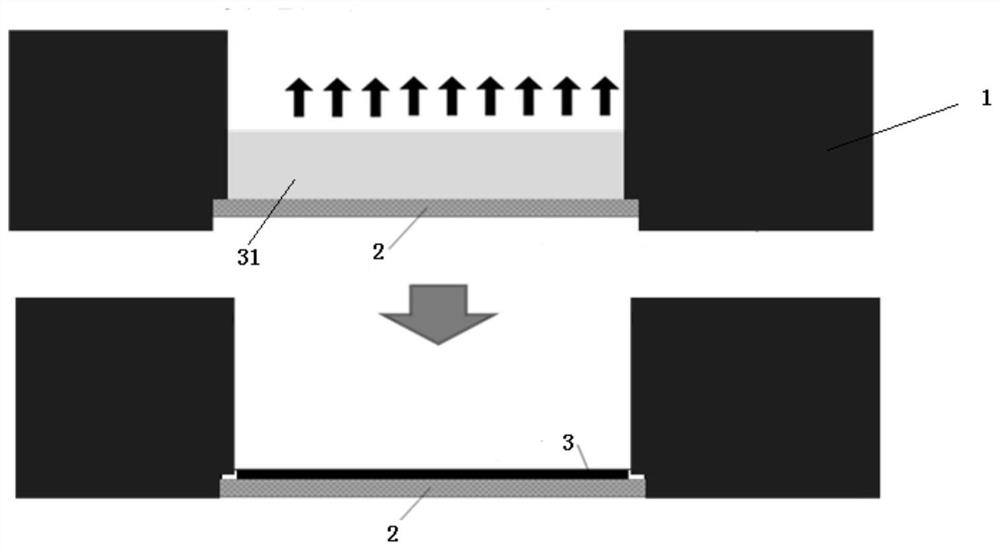
[0047] The process of sealing the air gap to be sealed by the insulating sheet-shaped two-dimensional material solution can be carried out in the following two ways:

[0048] The first way is to use the method of multiple spin coating, that is, the graphene oxide solution is spin coated on the solid medium on both sides of the groove for many times, and after each spin coating, it will be dried quickly with a hot plate, and through multiple spin coating Form a film composed of graphene oxide above the groove, and remove the solvent in the film with a long-time (for example 30min) heat treatment after multiple spin coatings, so that the film composed of graphene oxide becomes more stable; thus Seal the groove to create an air gap.

[0049] The second method adopts the immersion film forming method, that is, the solid medium containing the above-mentioned grooves is immersed in the graphene oxide solution, and the solvent is evaporated by slow heating, thereby forming graphite o...

Embodiment 2

[0054] Please refer to the attached Figure 3-6 , the concrete method of forming the air gap between metals comprises the following steps:

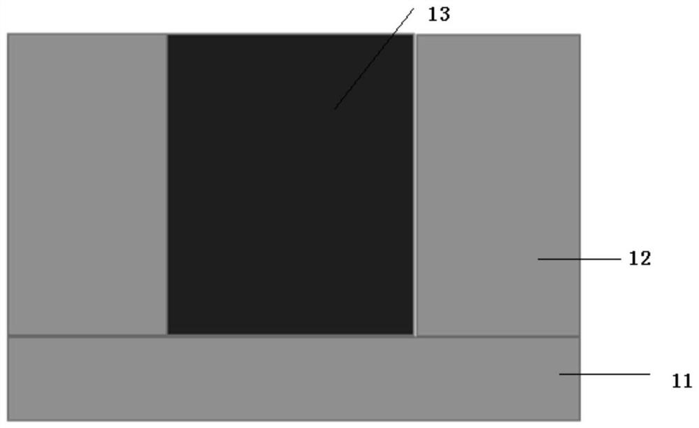
[0055] S01: Please refer to the attached image 3 The metal layer 12 and the isolation dielectric layer 13 are deposited on the silicon wafer 11 at the same time, and the isolation dielectric layer 13 and the metal layer 12 have a high selectivity etching coefficient.

[0056] S02: Please refer to the attached Figure 4 , using a dielectric etching process to remove the isolation dielectric layer 13, because the metal layer 12 and the isolation dielectric layer 13 have a high selectivity ratio, the metal layer 12 remains basically unchanged, thereby forming grooves between the metal layers.

[0057] S03: Please refer to the attached Figure 5 A layer of dielectric protection layer 14 is deposited on the upper surface and side walls of the metal layer 12; the function of the dielectric protection layer is to protect the metal layer from...

Embodiment 3

[0062] Please refer to the attached Figure 8, the specific method of forming the air gap between insulating dielectric layers is as follows: after forming the intermetallic air gap 17 in embodiment 2, deposit an insulating dielectric layer 16 on the thin film composed of insulating sheet-like two-dimensional material, so that the intermetallic air gap 17 is staggered The insulating medium layer is etched at the position, and stops on the thin film composed of insulating sheet-like two-dimensional material to form a groove between the insulating medium layers, and the insulating sheet-like two-dimensional material solution is coated on the insulating medium layer to form a A thin film composed of insulating sheet-like two-dimensional material on the groove forms an air gap 18 between insulating dielectric layers sealed with insulating sheet-like two-dimensional material. The specific method of coating the insulating sheet-like two-dimensional material is as described in Exampl...


PUM


Abstract

The invention discloses a method for forming an air gap, which includes the following steps: S01: forming a groove between solid media; S02: preparing an insulating sheet-like two-dimensional material, wherein the insulating sheet-like two-dimensional material includes insulating Sheet-like layer, the size of the insulating sheet-like layer in the sheet-like two-dimensional direction is larger than the size of the above-mentioned groove; S03: deposit the insulating sheet-like two-dimensional material on the solid medium and the groove; S04: for the solid Annealing the dielectric and the insulating sheet-like two-dimensional material to form a stable thin film composed of the insulating sheet-like two-dimensional material on the groove. The method for forming an air gap provided by the present invention can effectively increase the formation ratio of the air gap, thereby greatly reducing the effective dielectric constant and interconnection delay, further reducing costs and improving product performance.

Description

technical field [0001] The invention relates to the field of air gaps, in particular to a method for forming an air gap. Background technique [0002] In the process development of VLSI, due to the improvement of chip speed and the reduction of power consumption, etc., the delay of metal interconnection lines has far exceeded the delay of devices. In order to reduce interconnection delays, low dielectric constant materials are required. Since the relative nodal constant of air is 1, the ultimate means to reduce the dielectric constant is to achieve an air gap. [0003] The traditional air-gap interconnection technology scheme is to form the groove between the metal interconnection lines by photolithography after the interconnection is formed, and then deposit the dielectric medium by non-conformal chemical vapor deposition (CVD) and other film-forming techniques. The film seals the groove, forming a sealed air gap between the interconnects. Traditional solutions have the ...

Claims


Application Information

Patent Timeline
Patent Type & Authority Patents(China)
IPC IPC(8): H01L21/764
CPCH01L21/764H01L21/7682H01L21/02112H01L21/02282H01L21/76289H01L29/0649
Inventor 康晓旭沈若曦钟晓兰
Owner SHANGHAI INTEGRATED CIRCUIT RES & DEV CENT
Why Eureka
Try Eureka