
3d NAND flash memory device and its preparation method of coated silicon nanotube

A technology of silicon nanotubes and flash memory devices, applied in the field of 3DNAND flash memory, can solve the problems of restricting the manufacturing cost of 3DNAND, complicated process of cladding nanotubes, difficulty in time-consuming growth, etc., so as to reduce the steps of preparation and photolithography masks, The effect of controllable wall thickness and high verticality

Active Publication Date: 2021-06-11
HUAZHONG UNIV OF SCI & TECH
View PDF0 Cites 0 Cited by
  • Summary
  • Abstract
  • Description
  • Claims
  • Application Information

AI Technical Summary

Problems solved by technology

[0003] 3D NAND (that is, NAND) storage string was first disclosed in 2001 (“Novel Ultra High Density Memory with a Stacked-Surrounding Gate Transistor (S-SGT) Structured Cell”, IEDM Proc. (2001) 33-36), but this The active region of this three-dimensional NAND storage string is prepared by repeatedly forming sidewall isolation layers and etching the substrate, which requires strict operation, time-consuming, difficult growth and high cost.
[0004] The core component of the active region of vertical 3D NAND is coated nanotubes. Due to the complex process and poor controllability of the coated nanotubes prepared by the existing repeated deposition and etching processes, it has also become a constraint on the manufacturing cost of 3D NAND. Key factor

Method used


Image

  • 3d NAND flash memory device and its preparation method of coated silicon nanotube
  • 3d NAND flash memory device and its preparation method of coated silicon nanotube
  • 3d NAND flash memory device and its preparation method of coated silicon nanotube

Examples


Embodiment Construction

[0039] In order to make the object, technical solution and advantages of the present invention clearer, the present invention will be further described in detail below in conjunction with the accompanying drawings and embodiments. It should be understood that the specific embodiments described here are only used to explain the present invention, not to limit the present invention. In addition, the technical features involved in the various embodiments of the present invention described below can be combined with each other as long as they do not constitute a conflict with each other.

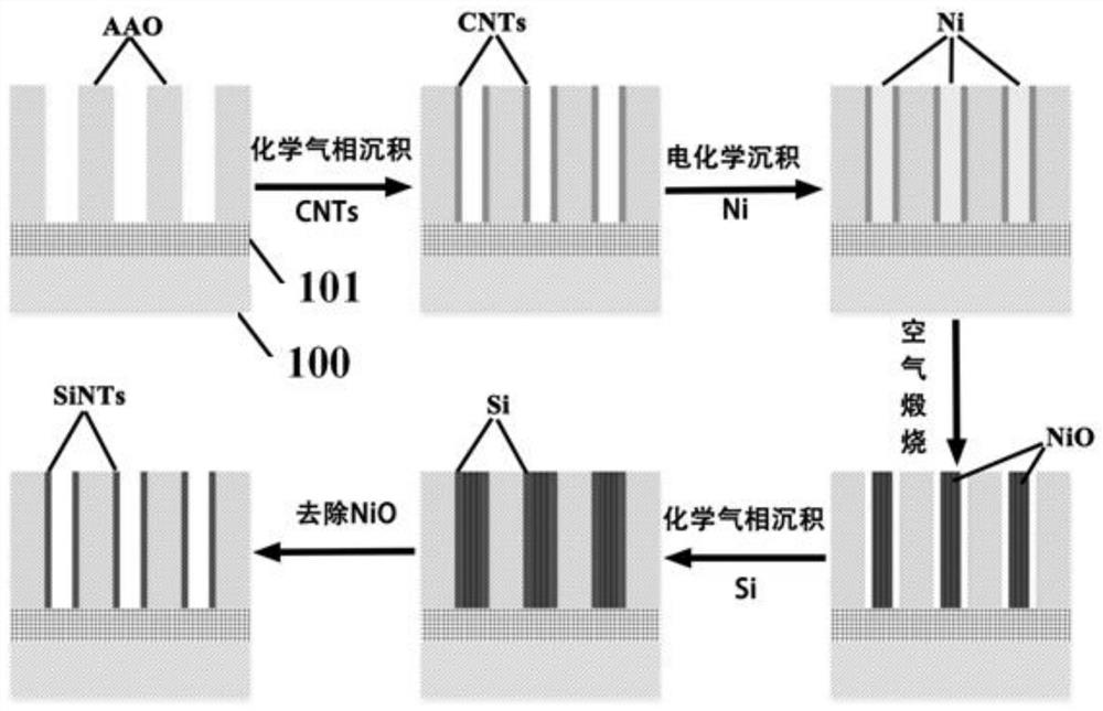
[0040] Such as figure 1 As shown, the preferred method of preparing coated silicon nanotubes of the present invention comprises the following steps:

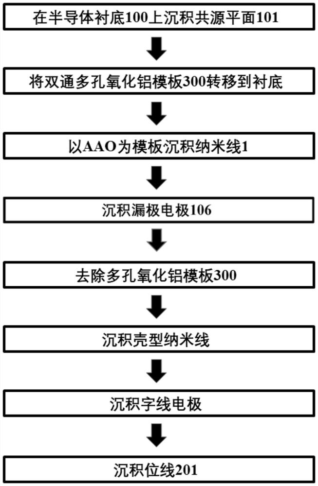
[0041] (1) Deposit a common source plane 101 on the substrate 100, and prepare a double-pass porous alumina template on the common source plane 101; The inside of the hole is deposited by thermal decomposition of acetylene, and the temperature o...


PUM


Abstract

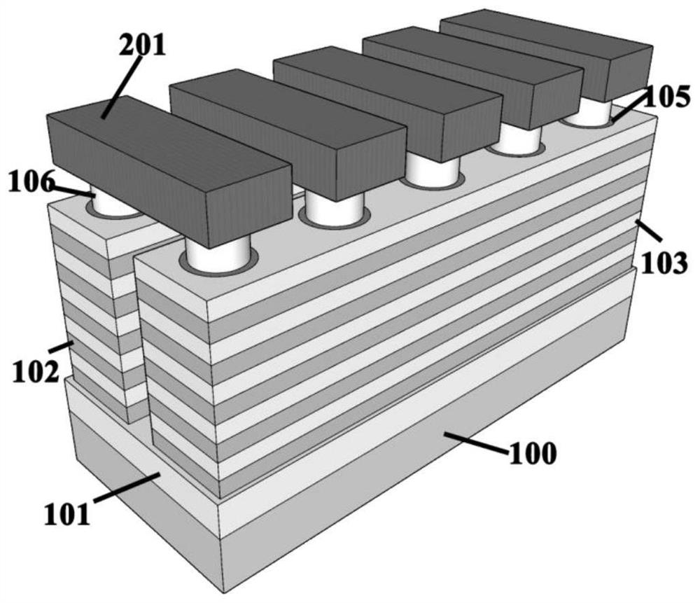
The invention discloses a 3D NAND flash memory device and a method for preparing the coated silicon nanotube, belonging to the field of 3D NAND flash memory. The preparation method of the coated silicon nanotube The storage device uses carbon nanotubes as templates, deposits a Ni layer in the inner cavity of the carbon nanotubes, then calcines the carbon nanotubes to remove the Ni layer and oxidizes the Ni layer to obtain NiO nanowires, and then uses chemical Vapor deposition deposits a Si layer outside the NiO nanowires, and finally removes the NiO nanowires to obtain coated silicon nanotubes. The 3D NAND flash memory device is composed of coated nanotubes as NAND strings, which can effectively simplify the device structure, reduce the complex manufacturing process steps in the original device manufacturing process, simplify the preparation process, and have a positive effect on reducing manufacturing costs. At the same time, the use of the multi-step template replication method makes the diameter and wall of the prepared nanotube more uniform, and the thickness of the tube wall is more controllable.

Description

technical field [0001] The invention belongs to the field of 3D NAND flash memory, and more specifically relates to a 3D NAND flash memory device and a method for preparing a coated silicon nanotube. Background technique [0002] Although 20nm (or smaller) polysilicon floating gate nonvolatile memory arrays have perfect manufacturing technology, in order to further increase integration and increase storage density, it is often necessary to continue to reduce the feature size of planar memory arrays (ie floating gate transistors Gate length), which puts higher requirements on the manufacturing process (such as photolithography, deposition technology, etc.), and the existing manufacturing process is difficult to support the continuous reduction of the feature size of the planar memory array. On the other hand, the further reduction of the feature size will also cause problems such as mutual crosstalk between adjacent cells and too few electrons stored in the floating gate in t...

Claims


Application Information

Patent Timeline
Patent Type & Authority Patents(China)
IPC IPC(8): H01L27/1157H01L27/11578H01L27/1158B82Y40/00H10B43/35H10B43/20H10B43/23
CPCB82Y40/00H10B43/23H10B43/20H10B43/35
Inventor 缪向水王升童浩
Owner HUAZHONG UNIV OF SCI & TECH
Learn More