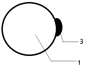
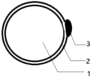
Nano semiconductor photocatalyst and preparation method thereof
A nano-semiconductor and photocatalyst technology, applied in chemical instruments and methods, physical/chemical process catalysts, metal/metal oxide/metal hydroxide catalysts, etc., can solve the problem of intensifying photogenerated electron-hole recombination and reducing photogenerated charges Separation efficiency, high energy consumption of interfacial charge transfer, etc., to improve photocatalytic performance, promote interfacial charge transfer, and reduce charge recombination
- Summary
- Abstract
- Description
- Claims
- Application Information
AI Technical Summary
Problems solved by technology
Method used
Image
Examples
Embodiment 1
[0037] Example 1: CdS|CdS(t)
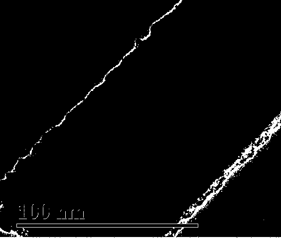
[0038]The CdS nanorod photocatalyst was ultrasonically dispersed in deionized water to form a dispersion with a solid content of 1.5 g / L, which was magnetically stirred at 60°C for 5 hours; the prepared cadmium acetate solution with a concentration of 0.25 mol / L was added drop by drop Add it to the dispersion liquid at a drop rate of 30 s / mL, stir for 2 hours, centrifuge, wash with deionized water three times to remove excess cadmium ions. Add the prepared sodium sulfide solution with a concentration of 0.5 mol / L to the cadmium sulfide nanorod dispersion that has adsorbed cadmium ions dropwise at a rate of 30 s / mL. After stirring for 1 hour, centrifuge and separate the obtained solid The material was washed and centrifuged multiple times with ethanol and water. Put the obtained yellow solid substance into a vacuum drying oven and keep it at 60° C. for 12 hours, and finally obtain a CdS nanorod photocatalytic material with an ultra-thin CdS elect...
Embodiment 2
[0040] Example 2: TiO 2 |TiO 2 ( t )
[0041] Anatase TiO 2 The nanoparticle photocatalyst was dispersed in isopropanol solvent, and ultrasonically dispersed for 3 hours to form a dispersion liquid with a solid content of 500 mg / L; after keeping at room temperature for 1 hour, 1 mol / L isopropyl titanate solution Add drop by drop, control the drop rate to 50s / mL, pour into a 100mL polytetrafluoroethylene sleeve; put the sealed polytetrafluoroethylene sleeve into a 100ml stainless steel reaction kettle, heat to 160°C, keep for 6 hours, and then cool naturally ; The suspension after the reaction was subjected to high-speed centrifugation, and ultrasonically cleaned several times with absolute ethanol and deionized water; the washed solid matter was placed in a vacuum drying oven and kept at 60°C for 12 hours, and finally the surface TiO 2 TiO with electronic intermediary layer 2 Nanophotocatalyst.
[0042] Disperse 20 mg of the prepared photocatalyst in 200 ml of water, con...
Embodiment 3
[0043] Example 3: BiVO 4 |CdS( t )
[0044] BiVO 4 Nanosheet photocatalyst, ultrasonically dispersed in deionized water to form a dispersion with a solid content of 50g / L, and magnetically stirred at 90°C for 3h; the prepared cadmium nitrate solution with a concentration of 0.5 mol / L was added dropwise to the dispersion solution, control the drop rate to 30 s / mL, stir for 3 hours, centrifuge, wash with deionized water three times to remove excess cadmium ions. Add the prepared sodium sulfide solution with a concentration of 1.0 mmol / L dropwise to the cadmium sulfide nanorod dispersion that has adsorbed cadmium ions, control the drop rate to 30 s / mL, keep it for 3 hours, and then centrifuge to separate the obtained solid The material was washed several times with ether and water. Put the obtained yellow solid substance in a vacuum drying oven and keep it at 60°C for 12 hours, and finally obtain BiVO with an ultra-thin CdS electron mediator layer on the surface. 4 Nanoshee...
PUM
| Property | Measurement | Unit |
|---|---|---|
| thickness | aaaaa | aaaaa |
| solid content | aaaaa | aaaaa |
Abstract
Description
Claims
Application Information
 - R&D
- Intellectual Property
- Life Sciences
- Materials
- Tech Scout
- Unparalleled Data Quality
- Higher Quality Content
- 60% Fewer Hallucinations
Browse by: Latest US Patents, China's latest patents, Technical Efficacy Thesaurus, Application Domain, Technology Topic, Popular Technical Reports.
© 2025 PatSnap. All rights reserved.Legal|Privacy policy|Modern Slavery Act Transparency Statement|Sitemap|About US| Contact US: help@patsnap.com


