Serially connected type perovskite/homojunction silicon laminated solar cell and preparation method thereof

A technology of solar cells and perovskite, applied in the field of solar cells, can solve the problem of high preparation cost

Pending Publication Date: 2019-09-17
深圳黑晶光电技术有限公司
View PDF0 Cites 19 Cited by
  • Summary
  • Abstract
  • Description
  • Claims
  • Application Information

AI Technical Summary

Problems solved by technology

At present, most of the tandem perovskite crystalline silicon stacks reported mainly stack perovskite solar cells and heterojunction silicon solar

Method used


Image

  • Serially connected type perovskite/homojunction silicon laminated solar cell and preparation method thereof

Examples


preparation example Construction

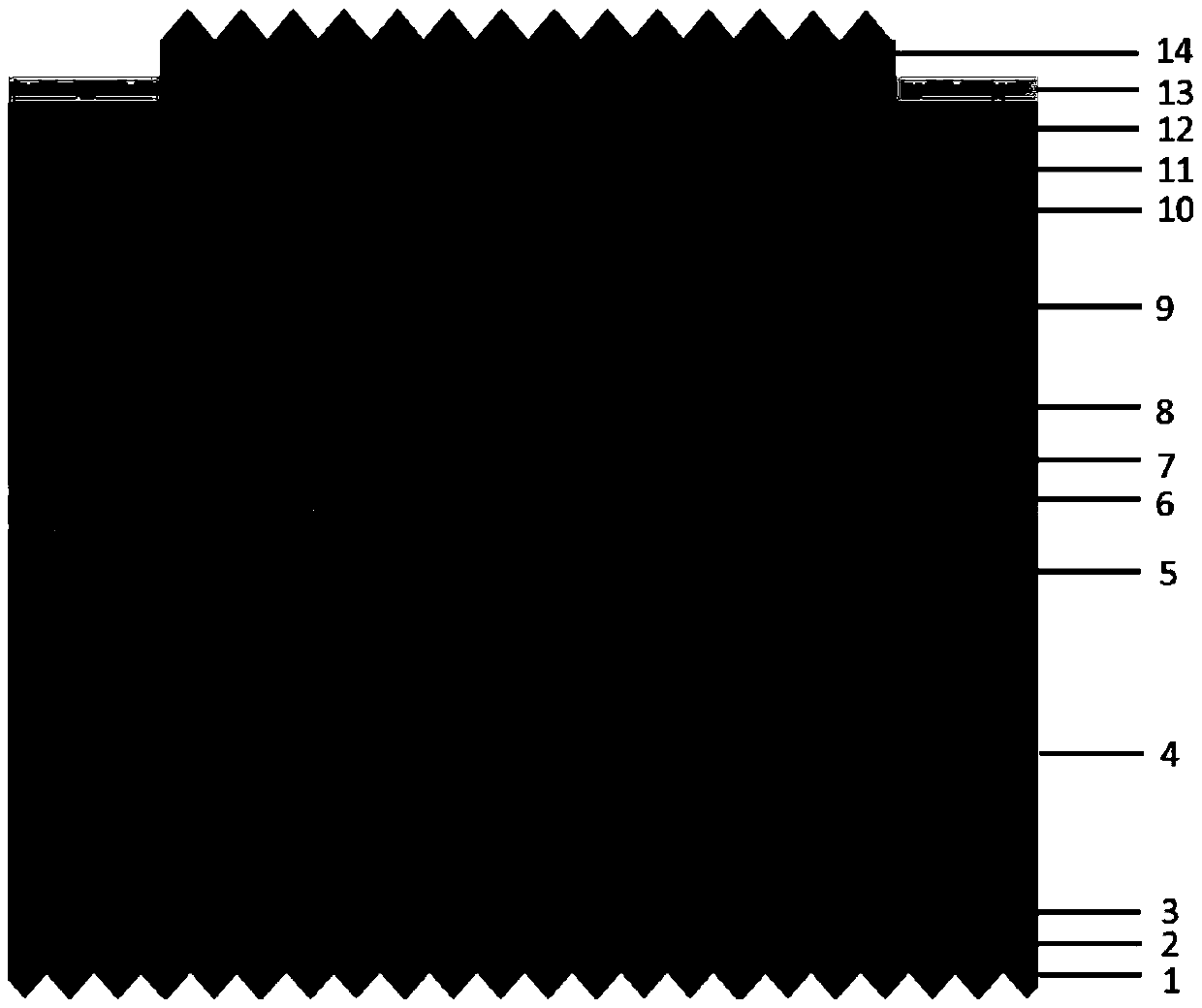
[0053] The invention provides a method for preparing a tandem perovskite / homojunction silicon laminated solar cell comprising the following steps:

[0054] Step 1: Texturing the surface of n-type silicon 4 with but not limited to alkaline solution.

[0055] Step 2: using but not limited to phosphorous compound to partially or fully diffuse phosphorous on the back of the silicon to form a heavily doped junction to form a partial or all n-type heavily doped layer 3 .

[0056] Step 3: Using but not limited to tubular boron diffusion or chain boron diffusion to expand boron on the front of the battery to form a p-type heavily doped emitter 5 .

[0057] Step 4: using but not limited to thermal growth, atomic deposition (ALD) or plasma enhanced chemical vapor deposition (PECVD) to prepare a bottom electrode passivation layer on the silicon backside.

[0058] Step 5: using but not limited to the method of opening holes by laser etching to make holes in the bottom electrode to prepar...

Embodiment 1

[0071] In this embodiment, silver electrode / n+ / SiO 2 / n-type silicon / p+ / SnO 2 / Perovskite light-absorbing layer / Spiro-OMeTAD / Ultra-thin Cu / Ag metal electrode structure to prepare tandem perovskite / homojunction silicon tandem solar cells.

[0072] The specific preparation process is as follows: adopt the n-type silicon wafer 4 with a resistivity of 5 ohm-cm prepared by the suspension zone melting method; use alkali to make texture on the back of the n-type silicon wafer; Type heavily doped layer 3; positive boron expansion to form pn homojunction to form p-type heavily doped emitter 5, junction depth 2μm; silicon cell surface prepared by thermal growth method SiO 2 After the ultra-thin passivation layer, local opening is performed to prepare the bottom electrode opening passivation layer 2; finally, a 1-micron silver electrode is evaporated to prepare the metal bottom electrode 1; the front surface of the silicon wafer is directly treated with ozone to obtain ultra-thin SiO 2...

Embodiment 2

[0074] In this embodiment, silver electrode / n+ / SiO 2 / n-type silicon / p+ / SiO 2 / SnO 2 / Perovskite Light Absorbing Layer / Spiro-OMeTAD / MoO x / ITO / Ag gate electrode / MgF 2 Structure preparation of tandem perovskite / homojunction silicon tandem solar cells.

[0075]The specific preparation process is as follows: adopt the n-type silicon wafer 4 with a resistivity of 5 ohm-cm prepared by the suspension zone melting method; use alkali to make texture on the back of the n-type silicon wafer; type heavily doped layer 3; the front side is expanded with boron to form a pn homojunction to form a p-type heavily doped emitter 5 with a junction depth of 3 μm; the silicon cell surface is prepared by thermal growth of SiO 2 After the ultra-thin passivation layer, local opening is performed to prepare the bottom electrode opening passivation layer 2; finally, a 1-micron silver electrode is evaporated to prepare the metal bottom electrode 1; the front surface of the silicon wafer is directly t...


PUM

PropertyMeasurementUnit
Thicknessaaaaaaaaaa
Thicknessaaaaaaaaaa
Thicknessaaaaaaaaaa

Abstract

The invention discloses a serially connected type perovskite/homojunction silicon laminated solar cell and a preparation method thereof. The laminated solar cell comprises an n-type homogeneous crystalline silicon solar cell serving as a bottom cell based on a PERC (passivated emitter rear contact cell) structure. A perovskite solar cell with a transparent electrode serves as a top cell. The structure of the laminated solar cell sequentially comprises a metal bottom electrode, a bottom electrode opened passivation layer, a local or all n-type heavily doped layer, n-type silicon, a p-type heavily doped emitter, an emitting electrode passivation layer, a tunneling layer, an electron transport layer, a perovskite absorption layer, a hole transport layer, a top electrode buffer layer, a transparent electrode, a metal grid line electrode and an antireflection film from bottom to top. The laminated solar cell is based on the mainstream homojunction PREC solar crystalline silicon cell in the current photovoltaic industry, and is simple in preparation process, low in preparation cost, high in light conversion efficiency and suitable for large-scale industrial production.

Description

technical field [0001] The invention relates to the technical field of solar cells, in particular to a stacked solar cell, in particular to a tandem perovskite / homojunction silicon stacked solar cell and a preparation method thereof. Background technique [0002] Solar energy has become the top priority in the development of new energy due to its inexhaustible, inexhaustible, pollution-free, noise-free, and easy-to-use advantages. Due to its high efficiency and cost close to grid parity, solar cells have become a very promising and competitive clean energy source. [0003] At present, among the photovoltaic cells, the main commercialized solar cells are silicon solar cells, which currently occupy the mainstream position in the market share. Since the theoretical limit photoelectric conversion efficiency of single-junction silicon solar cells is about 30%, the conversion efficiency of silicon solar cells currently on the market is about 22%, which is already close to the the...

Claims


Application Information

Patent Timeline
IPC IPC(8): H01L31/068H01L31/18H01L31/0216H01L51/42H01L51/48
CPCH01L31/068H01L31/1804H01L31/02168H10K30/00Y02E10/547Y02E10/549Y02P70/50
Inventor 郑将辉徐成易海芒
Owner 深圳黑晶光电技术有限公司
Why Eureka
Try Eureka