Dual-light emitting layer structure blue-light OLED and manufacturing process thereof

A technology of manufacturing process and light-emitting layer, which is applied in the field of blue light OLED, and achieves the effects of good feasibility and repeatability, simple manufacturing process and low cost

Inactive Publication Date: 2019-09-20
CHONGQING UNIV OF POSTS & TELECOMM
View PDF4 Cites 7 Cited by
  • Summary
  • Abstract
  • Description
  • Claims
  • Application Information

AI Technical Summary

Problems solved by technology

[0005] Aiming at the efficiency roll-off problem of the device, the present invention designs a blue-light OLED device with a simple structure and double-emitting layer structure. On the basis of the traditional OLED structure, the concentration gradient is generated by adding light-emitting lay...

Method used


Image

  • Dual-light emitting layer structure blue-light OLED and manufacturing process thereof
  • Dual-light emitting layer structure blue-light OLED and manufacturing process thereof
  • Dual-light emitting layer structure blue-light OLED and manufacturing process thereof

Examples


preparation example Construction

[0036] (2) Preparation of hole injection layer

[0037] Put the processed ITO glass substrate into the ultra-high vacuum vacuum evaporation chamber to prepare various functional layers, MoO 3 The evaporation rate is controlled at 0.3 Angstroms per second, and the duration is about 100 seconds;

[0038] (3) Preparation of hole transport layer and electron blocking layer

[0039] The hole injection material TAPC is heated to the evaporation temperature, the evaporation rate is controlled at 1 Angstrom per second, and the evaporation time is about 600 seconds;

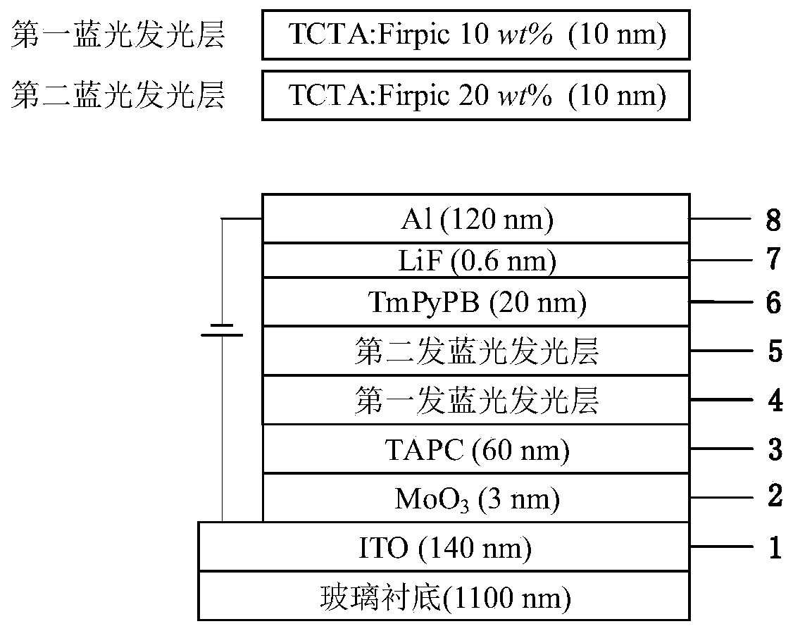
[0040] (4) Preparation of double light-emitting layers

[0041] Co-evaporation of host and guest materials is required when evaporating the light-emitting layer. The guest doping concentration and thickness of the light-emitting layer of the first blue light-emitting layer and the second blue light-emitting layer must satisfy the relationship of y≤0.5x, 5≤w≤30. In this example, the evaporation rate of TCTA in the first...

Embodiment 2

[0046] Embodiment 2 (comparative example):

[0047] Compared with the device of the invention, this comparative example has only one light-emitting layer, the doping concentration of the guest is the same as that of the first light-emitting layer of the device of the invention, and the thickness of the light-emitting layer is 2w, that is, 20. The rest of the structure is exactly the same. The comparison device structure is:

[0048] Comparative example device: Glass(1100nm) / ITO(140nm) / MoO 3 (3nm) / TAPC(60nm) / TCTA: Firpic(10%,20nm) / TmPyPB(20nm) / LiF(0.6nm) / Al(120nm);

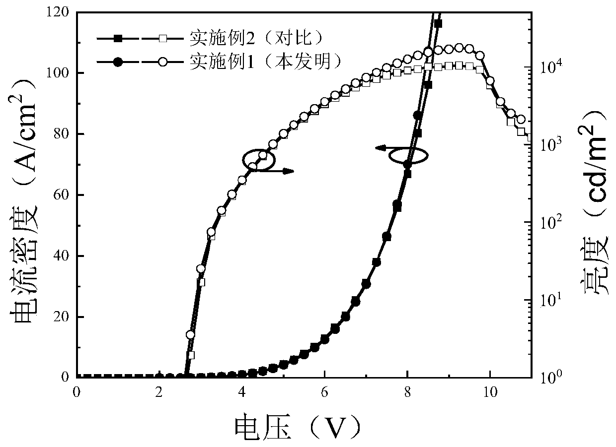
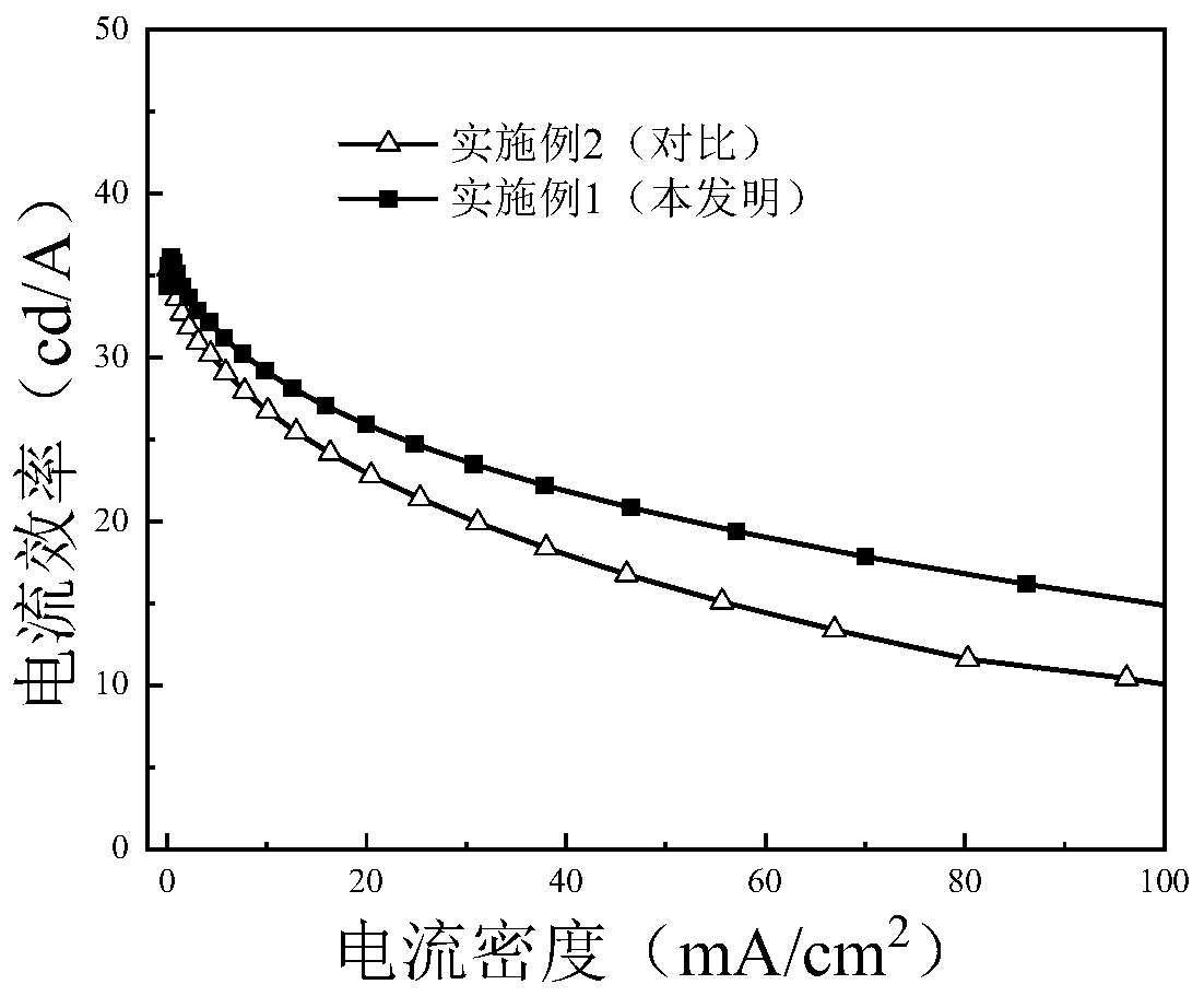
[0049] The comparison of performance parameters between the device embodiment 1 of the present invention and the comparative device embodiment 2 is shown in the table below.

[0050]

[0051] From the above data, it can be found that the light-up voltage and driving voltage of the device of the present invention (Example 1) are slightly lower than that of the comparative device (Example 2), and the maximum ef...


PUM

PropertyMeasurementUnit
Thicknessaaaaaaaaaa

Abstract

The invention requests and protects a dual-light emitting layer structure blue-light OLED device and a manufacturing process thereof. The device comprises a positive electrode substrate, a hole injection layer, a hole transmission layer, a first light-emitting layer, a second light-emitting layer, an electronic transmission layer, an electronic injection layer and a negative electrode, wherein the first light-emitting layer and the second light-emitting layer employ the same main body materials, same object material and same thickness, and the object doping concentration of the first light-emitting layer is not higher than 50% of the object doping concentration of the second light-emitting layer. The dual-light emitting layer structure provided by the technical scheme is simple, the exciton utilization rate and the composite region can be expanded, and the efficiency roll-off of the device is effectively improved.

Description

technical field [0001] The invention belongs to the field of LEDs, in particular to the blue-light OLED technology with a double-light-emitting layer structure. Background technique [0002] Organic light-emitting diodes (Organic Light-Emitting Diodes, OLEDs) have attracted widespread attention because of their huge application markets in the fields of display and lighting. Compared with other display technologies, OLED panels have many advantages, such as a wide range of material selection, full-color display in the 380nm-700nm spectral region, wide viewing angle, fast response speed, low driving voltage, and flexible display. It has been developed and applied rapidly in the past 20 years. OLED uses organic small molecule semiconductor materials as functional materials, and is driven by an external electric field to complete the transport and recombination of carriers to form excitons, and the excitons radiate to achieve light emission. Therefore, OLED is a current-driven...

Claims


Application Information

Patent Timeline
IPC IPC(8): H01L51/50H01L51/56
CPCH10K50/12H10K50/13H10K71/00
Inventor 王振陈爱谢嘉凤
Owner CHONGQING UNIV OF POSTS & TELECOMM
Why Eureka
Try Eureka