Method for preparing indium-aluminum-zinc oxide thin film transistor in low temperature environment

A technology of oxide film and low-temperature environment, which is applied in the manufacture of transistors, semiconductor devices, semiconductor/solid-state devices, etc., can solve the problems of long thermal annealing time, reduce device production efficiency, limit the application of flexible transparent circuits, etc., and achieve strong repeatability , excellent electrical properties, and the effect of shortening the preparation time

Active Publication Date: 2019-10-08
SHANDONG UNIV
View PDF3 Cites 3 Cited by
  • Summary
  • Abstract
  • Description
  • Claims
  • Application Information

AI Technical Summary

Problems solved by technology

[0008] In the prior art, there is a method of using radio frequency magnetron sputtering multi-component amorphous metal oxide thin film transistors, but this method has the following defects: (1) The thermal annealing temperature exceeds 200 ° C, which seriously limits its application in flexible transparent circuits. (2) The thermal annealing time is longer, which greatly reduces the production efficiency of the device

Method used


Image

  • Method for preparing indium-aluminum-zinc oxide thin film transistor in low temperature environment
  • Method for preparing indium-aluminum-zinc oxide thin film transistor in low temperature environment
  • Method for preparing indium-aluminum-zinc oxide thin film transistor in low temperature environment

Examples


Embodiment 1

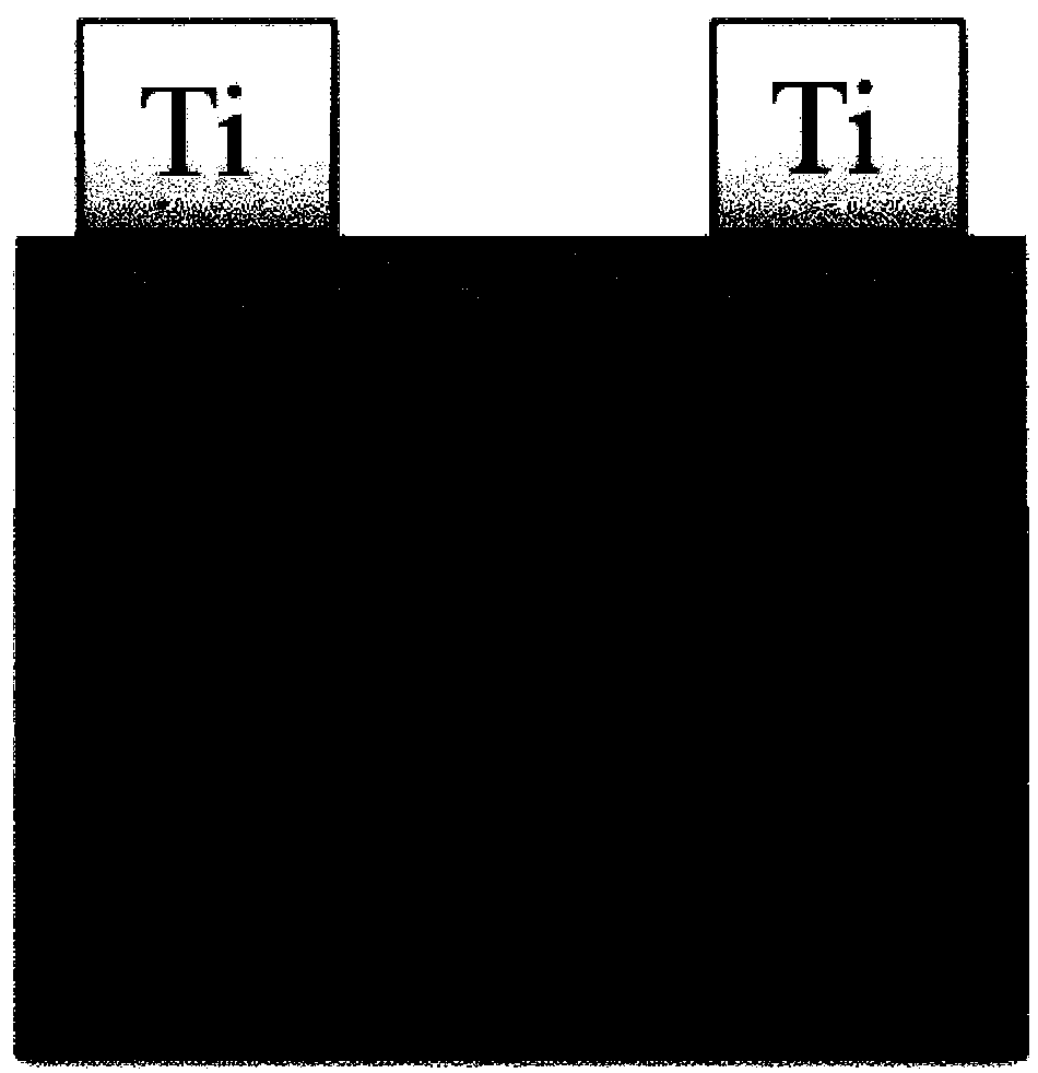
[0054] A method for preparing indium aluminum zinc oxide thin film transistors in a low temperature environment. A multi-element amorphous metal oxide thin film transistor includes a substrate, an IAZO active layer, a source electrode and a drain electrode, and a source electrode and a drain electrode from bottom to top. Grown on IAZO active layer, such as figure 2 As shown, the preparation method is carried out at a temperature of 20°C-70°C, and includes the following steps:

[0055] (1) Growing an IAZO film on a substrate to prepare the IAZO active layer;

[0056] (2) Turn on the UV-ozone power switch to make the UV-ozone work 3-5 minutes in advance; ensure that the UV-ozone chamber is relatively clean; the UV-ozone model is ProCleaner TM 220.

[0057] (3) Place the sample generated in step (1) in UV-ozone, the processing time is 3 minutes;

[0058] (4) Source and drain electrodes are grown on the surface of the IAZO active layer to obtain.

[0059] UV-ozone is a low-temperature tr...

Embodiment 2

[0061] According to the method of preparing an indium aluminum zinc oxide thin film transistor in a low temperature environment according to embodiment 1, the difference is that:

[0062] In step (1), the IAZO thin film is grown on the substrate by the radio frequency magnetron sputtering method to obtain the IAZO active layer, including the following steps:

[0063] A. Open the door of the RF magnetron sputtering chamber, put in the substrate and IAZO ceramic target, and close the chamber door;

[0064] B. Vacuum until the vacuum degree in the chamber is lower than 1×10 -5 Torr;

[0065] C. Pour high-purity Ar into the chamber, stop charging after 1 minute, and repeat this operation 3 times;

[0066] D. Set the sputtering power to 90W, pass in high-purity Ar, adjust the gas flow rate to 20SCCM, and keep the indoor working pressure at 3.68mTorr;

[0067] E. Sputtering for 13 minutes and 20 seconds, turn off the sputtering power supply;

[0068] F. After waiting for 30 minutes, take out th...

Embodiment 3

[0082] According to the method of preparing an indium aluminum zinc oxide thin film transistor in a low temperature environment according to embodiment 1, the difference is that:

[0083] In step (3), the processing time is 15 minutes.


PUM

PropertyMeasurementUnit
thicknessaaaaaaaaaa
thicknessaaaaaaaaaa
surface roughnessaaaaaaaaaa

Abstract

The invention relates to a method for preparing an indium-aluminum-zinc oxide thin film transistor in a low temperature environment. The multi-element amorphous metal oxide thin film transistor sequentially comprises a substrate, an IAZO active layer, a source electrode and a drain electrode from bottom to top, wherein the source electrode and the drain electrode are grown on the IAZO active layer. The preparation method is carried out at a temperature ranging between 20 DEG C and 70 DEG C and includes the steps of (1) growing an IAZO film on a substrate to prepare an IAZO active layer; (2) placing the generated device in UV-ozone, wherein the processing time is 5 minutes; and (3) growing a source electrode and a drain electrode on the surface of the IAZO active layer so as to obtain the indium-aluminum-zinc oxide thin film transistor. The high-performance IAZO TFT is prepared in the low temperature environment through exploring the optimizing the treatment carried out by UV-ozone on the IAZO active layer.

Description

Technical field [0001] The invention relates to a method for preparing an indium aluminum zinc oxide thin film transistor in a low temperature environment, and belongs to the technical field of semiconductor materials and devices. Background technique [0002] With the rapid development of flat panel display technology, thin film transistors (TFTs), as the core components of display switches and driving units, have also been put forward with higher standards, such as higher mobility, lower preparation temperature, and higher The transparency and flexibility. However, silicon-based TFTs, which are currently the most widely used in the display field, can no longer meet the above requirements. This is mainly because the silicon-based TFT itself has many difficult to solve problems, such as the low mobility of hydrogenated amorphous silicon TFT, and the high preparation temperature of polysilicon TFT. [0003] In recent years, amorphous oxide semiconductor (AOS) has begun to be appli...

Claims


Application Information

Patent Timeline
Patent Type & Authority Applications(China)
IPC IPC(8): H01L21/34H01L21/02H01L29/10H01L29/417H01L29/45H01L29/786
CPCH01L29/66969H01L21/02565H01L21/02664H01L21/02057H01L29/45H01L21/02631H01L21/02381H01L29/41733H01L29/1033H01L29/78696H01L29/7869
Inventor 冯先进徐伟东
Owner SHANDONG UNIV
Why Eureka
Try Eureka