

Photoelectric material with CuO nanoparticle modified ZnO nanowire array, preparation and application
A nanowire array and nanoparticle technology, applied in the field of nanomaterials, can solve the problems of low light absorption and utilization, and achieve the effects of increasing carrier concentration, high yield, and increasing lifespan
- Summary
- Abstract
- Description
- Claims
- Application Information
AI Technical Summary
Problems solved by technology
Method used
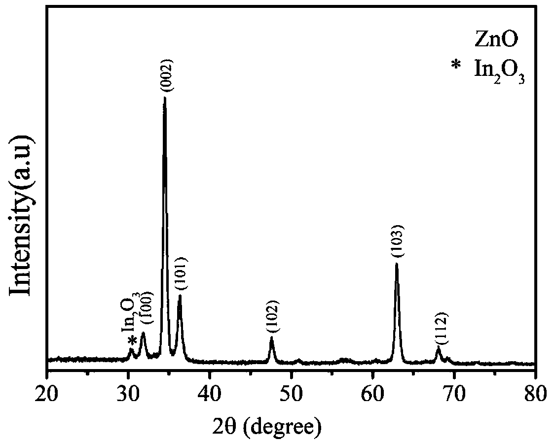
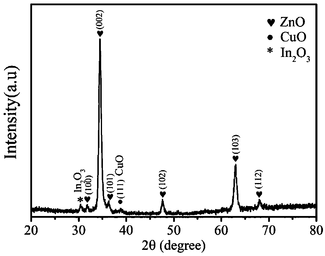
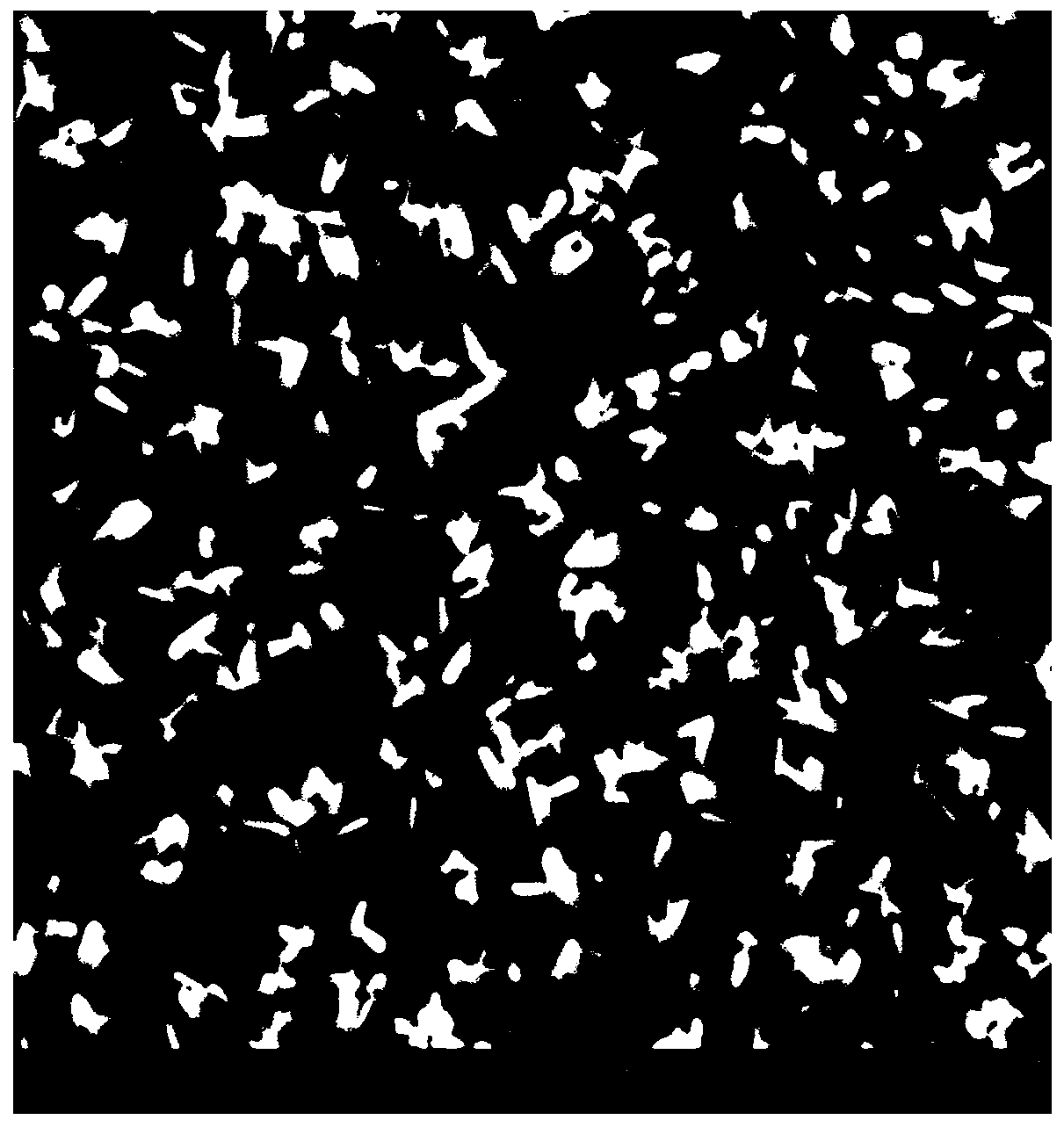
Image

Examples
Embodiment 1
[0045] Step 1: Preparation of ZnO seed layer:
[0046] Weigh 3.8413g, 0.35mol / L of Zn(CH 3 COOH) 2 2H 2 Pour O into a beaker, then pour 50mL of ethanol, stir at room temperature for 30min, measure 1.2mL of ethanolamine and slowly add it into the solution, continue to stir for about 30min or more to form a transparent and uniform solution, and put the resulting solution in an oven at 75°C After sinking for 5 hours, a transparent and uniform sol was obtained. Afterwards, the ITO substrate was spin-coated at a gradual speed of 800 rpm, 2000 rpm, and 3500 rpm in turn. The spin-coating time was about 5 seconds at each rpm, and repeated 4 times. All heat treatment was carried out by placing the ITO substrate in an oven at 80°C for 5h. After the spin coating, the ITO substrate was annealed in a muffle furnace, the temperature was raised to 400° C., and the temperature was kept for 90 minutes to prepare the ZnO seed layer.
[0047] Step 2: Preparation of ZnO nanowire arrays:
[...
Embodiment 2
[0055] The difference between this embodiment and embodiment 1 is that in the step 1, the annealing temperature of the ITO substrate in the muffle furnace is 350°C.
[0056] The morphology and properties of the photoelectric composite material prepared in this example are the same as those in Example 1.
Embodiment 3
[0058] The difference between this embodiment and embodiment 1 is that the annealing temperature of the ITO substrate on which the ZnO nanowire array is grown in the step 3 in the muffle furnace is 300° C.
[0059] The morphology and properties of the photoelectric composite material prepared in this example are the same as those in Example 1.
PUM
| Property | Measurement | Unit |
|---|---|---|
| Length | aaaaa | aaaaa |
| Diameter | aaaaa | aaaaa |
| Diameter | aaaaa | aaaaa |
Abstract
Description
Claims
Application Information