Miniature wide-spectrum and high-sensitivity graphene fiber photoelectric detection chip

A photoelectric detection and graphene technology, applied in the field of optical fiber communication, can solve the problems of slow response speed of photoelectric detection chips, low detection efficiency, complicated manufacturing process, etc., so as to improve photoelectric detection efficiency, stabilize photoelectric detection sensitivity and compact chip structure. Effect

Active Publication Date: 2019-10-25
JINAN UNIVERSITY
View PDF11 Cites 2 Cited by
  • Summary
  • Abstract
  • Description
  • Claims
  • Application Information

AI Technical Summary

Problems solved by technology

[0006] The present invention aims at overcoming at least one deficiency of the above-mentioned prior art, and provides a miniature wide-spectrum high-sensitivity graphene optical fiber photodetection chip, which is used to solve the problems of slow response speed, low stability, and manufacturing process of photodetection chips in the prior art. Complexity, low detection efficiency, and low sensitivity

Method used


Image

  • Miniature wide-spectrum and high-sensitivity graphene fiber photoelectric detection chip
  • Miniature wide-spectrum and high-sensitivity graphene fiber photoelectric detection chip
  • Miniature wide-spectrum and high-sensitivity graphene fiber photoelectric detection chip

Examples


Embodiment

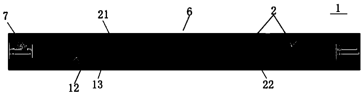
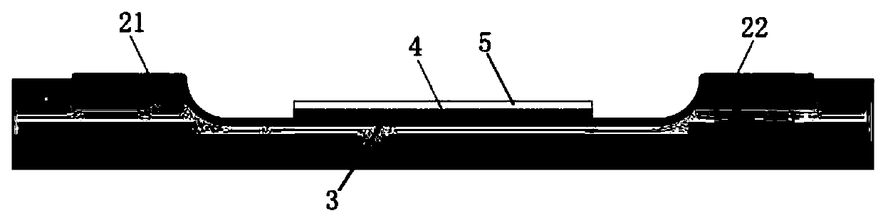
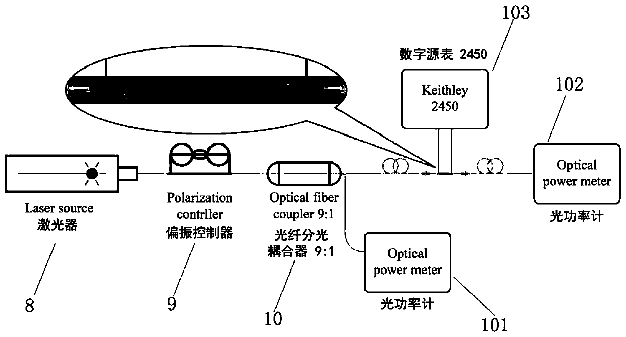
[0042] Such as Figure 1~2 As shown, the present embodiment includes a side-polished optical fiber 1, a microstrip electrode 2, a graphene film 3, a PB film 4, and a PMMA film 5, and the side-polished optical fiber 1 includes a cladding 12, a core 13, and a cladding 12 and the fiber core 13 are partially polished to form a polishing zone 6; the microstrip electrode 2 covers both sides of the fiber core 13 in the polishing zone 6 and extends to the non-polishing zone 7; the upper surface of the microstrip electrode 2 The surface is covered with PMMA film 5, PB film 4, and graphene film 3 sequentially from top to bottom, and the three film layers form a PMMA-PB-graphene composite film.

[0043] The microstrip electrode 2 includes a first metal electrode 21 and a second metal electrode 22, the first metal electrode 21 and the second metal electrode 22 are symmetrically distributed on both sides of the fiber core 13, covering the polishing area 6 and the non-polishing area 7 on. ...


PUM

PropertyMeasurementUnit
thicknessaaaaaaaaaa
thicknessaaaaaaaaaa
thicknessaaaaaaaaaa

Abstract

The invention discloses a miniature wide-spectrum and high-sensitivity graphene fiber photoelectric detection chip. The miniature wide-spectrum and high-sensitivity graphene fiber photoelectric detection chip comprises a side polishing fiber, microstrip electrodes, a graphene thin film, a PB thin film and a PMMA thin film, wherein the side polishing fiber comprises a fiber core and a coating layer, the coating layer and the fiber core are partially polished to form a polishing region, the polishing region of the side polishing fiber faces upwards, the microstrip electrodes are arranged at twosides of the fiber core and cover non-polishing regions, and the PMMA thin film, the PB thin film and the graphene thin film sequentially cover upper surfaces of the microstrip electrodes from top tobottom. The chip has the characteristics of rapid response speed, high detection efficiency, high stability and excellent photoelectric detection performance; an all-fiber structure is employed and isperfectly compatible with a fiber communication system, and the problem of compatibility in production is solved; and the chip is directly fabricated on the fiber, the fabrication process is simple,mass production is facilitated, the problem of coupling of the fiber and a waveguide structure is also solved, the insertion loss is reduced, and the device integration is improved.

Description

technical field [0001] The invention relates to the technical field of optical fiber communication, and more specifically, relates to a miniature wide-spectrum high-sensitivity graphene optical fiber photodetection chip. Background technique [0002] With the rapid development of optical communication networks, photoelectric detection and sensing technologies are becoming more and more mature, and higher requirements are placed on the sensitivity, response speed, and applicable wavelength range of photodetectors. The rapid development of CMOS technology promotes the development of photodetectors in the direction of integration. At the same time, the development of all-optical communication networks also puts forward the demand for all-fiber photodetector chips. [0003] Graphene, as a new type of thin film material, is almost completely transparent, absorbs only 2.3% of light, and can absorb energy in a wide spectral range to generate electron-hole pairs, enabling wide bands...

Claims


Application Information

Patent Timeline
Patent Type & Authority Applications(China)
IPC IPC(8): G02B6/42H01L31/08
CPCG02B6/4298H01L31/08
Inventor 朱文国余健辉陈哲卓琳青林艳梅郑华丹李志斌
Owner JINAN UNIVERSITY
Why Eureka
Try Eureka