Si-APD photoelectric detector based on black silicon and quantum dots and preparation method of Si-APD photoelectric detector

A technology of photodetectors and quantum dots, which is applied in circuits, electrical components, semiconductor devices, etc., can solve the problems of small over-noise, inability to respond to near-infrared bands, and low near-infrared responsivity, achieving long response time and improving infrared Responsiveness, effect of improving absorption efficiency

Pending Publication Date: 2019-11-05
CHONGQING INST OF GREEN & INTELLIGENT TECH CHINESE ACADEMY OF SCI
View PDF0 Cites 2 Cited by
  • Summary
  • Abstract
  • Description
  • Claims
  • Application Information

AI Technical Summary

Problems solved by technology

[0006] Based on the problems existing in the prior art, the present invention provides a Si-APD photodetector based on black silicon and quantum dots and a preparation method thereof. The present invention uses the black silicon layer covered with quantum dots as the

Method used


Image

  • Si-APD photoelectric detector based on black silicon and quantum dots and preparation method of Si-APD photoelectric detector
  • Si-APD photoelectric detector based on black silicon and quantum dots and preparation method of Si-APD photoelectric detector
  • Si-APD photoelectric detector based on black silicon and quantum dots and preparation method of Si-APD photoelectric detector

Examples


Embodiment Construction

[0033] The following will clearly and completely describe the technical solutions in the embodiments of the present invention with reference to the drawings in the embodiments of the present invention. Apparently, the described embodiments are only some of the embodiments of the present invention, not all of them. Based on the embodiments of the present invention, all other embodiments obtained by persons of ordinary skill in the art without making creative efforts belong to the protection scope of the present invention. Additionally, the protection scope of the present invention should not be limited only to the specific experimental methods or specific parameters described below.

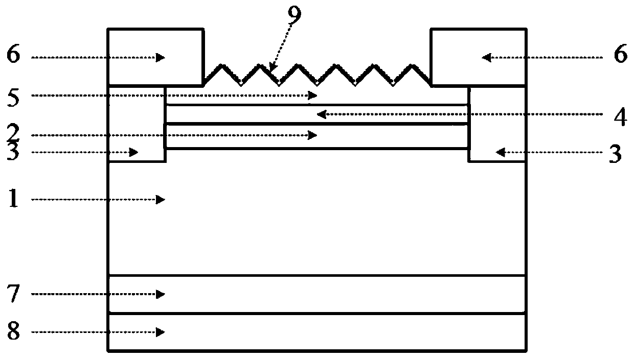
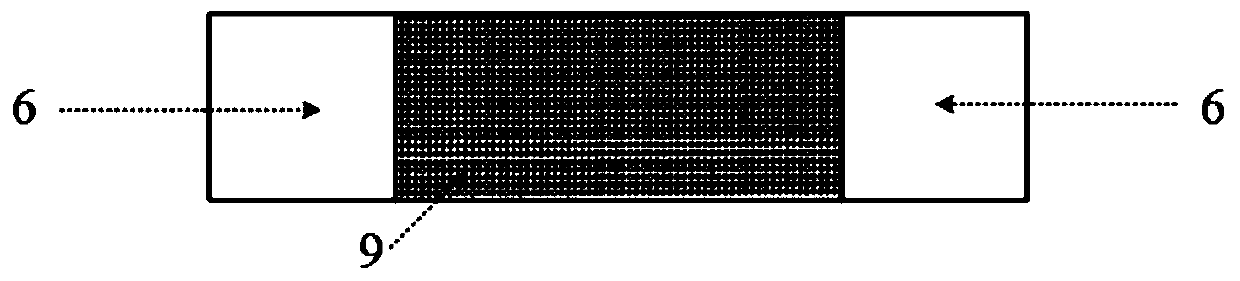
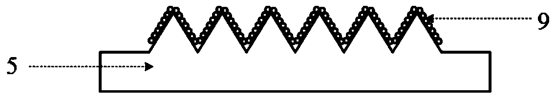
[0034] The applicant is committed to the research of expanding the detection spectrum of Si, and has carried out long-term development and exploration based on black silicon and quantum dots. The present invention provides a Si-APD photodetector based on black silicon and quantum dots and its prep...


PUM

PropertyMeasurementUnit
Diameteraaaaaaaaaa
Thicknessaaaaaaaaaa
Thicknessaaaaaaaaaa

Abstract

The invention discloses a Si-APD photoelectric detector based on black silicon and quantum dots and a preparation method of the Si-APD photoelectric detector. The Si-APD photoelectric detector comprises an intrinsic Si substrate (1); a P region (2) which is positioned above the center of the intrinsic Si substrate (1); protection ring regions, namely N regions (3), which are located above the twosides of the intrinsic Si substrate (1); an N+ region (4) which is positioned above the P region (2); an N+ black silicon layer (5) which is located above the N+ region (4); a quantum dot region (9) which is located on the upper surface of the N+ black silicon layer (5); a P+ region (7) which is located below the intrinsic Si substrate (1); an upper electrode (6) which is located on the quantum dot region (9) and the upper surface of the annular protection region N region (3); and a lower electrode (8). According to the invention, the black silicon layer covered with quantum dots is used as the photosensitive layer, and the high infrared absorption characteristic of the black silicon layer is utilized, so that the problems that a traditional Si-APD photoelectric detector cannot respond toa near infrared band or is low in near infrared responsivity and the like are solved; the Si-APD photoelectric detector can absorb near-infrared band light waves, and has the advantages of wide spectral response, high responsivity, low over-noise, low cost, easiness in processing and the like.

Description

technical field [0001] The invention belongs to the technical field of photoelectric detection, and specifically relates to a Si-APD photodetector based on black silicon and quantum dots and a preparation method thereof, which belongs to the photodetector structure and semiconductor nanomaterials in the technical field of silicon-based avalanche photodetectors. Background technique [0002] A photodetector is a photoelectric device that can convert light signals into electrical signals. It is characterized by small package size, fast photoelectric response, high detection sensitivity, mature technology and low price. Photoelectric detectors are widely used in signal transmission processing, infrared thermal imaging remote sensing, ray detection, industrial automatic control and other military and civilian fields. [0003] An avalanche photodiode (APD) is a photodetector with internal gain. It works at a high reverse bias voltage that can cause the device to undergo avalanche...

Claims


Application Information

Patent Timeline
IPC IPC(8): H01L31/0236H01L31/0288H01L31/032H01L31/0352H01L31/107H01L31/18
CPCH01L31/02366H01L31/0288H01L31/0324H01L31/035218H01L31/107H01L31/18
Inventor 陆文强张昆付勰康帅冯双龙
Owner CHONGQING INST OF GREEN & INTELLIGENT TECH CHINESE ACADEMY OF SCI
Why Eureka
Try Eureka