Global optimization design method of photoelectric imaging system based on computational imaging

An optoelectronic imaging and computational imaging technology, applied in computing, image enhancement, image analysis, etc., can solve the problems of lack of depth information, bulky optical system, high processing and assembly costs, and reduce the difficulty of design.

Pending Publication Date: 2019-11-15
XIDIAN UNIV
View PDF5 Cites 11 Cited by
  • Summary
  • Abstract
  • Description
  • Claims
  • Application Information

AI Technical Summary

Problems solved by technology

[0002] As a product of the industrial age, traditional photoelectric imaging can well meet the needs of traditional industries. At present, photoelectric imaging equipment generally has the following problems: the use of photoelectric imaging equipment is severely restricted by weather conditions; the optical system is bulky and heavy in photoelectric equipment. Heavy, high processing and assembly costs; defocus, motion blur and lack of depth information are difficult problems for optoelectronic imaging equipment
Common aberrations in the imaging process include spherical aberration, coma, field curvature, astigmatism, distortion and chromatic aberration, etc. In order to eliminate various order aberrations, a common solution in the design and processing of optical systems is to use multiple sets of mirrors Optimal design of groups and multi-lens lenses, and the use of expensive special materials such as fluorite for processing, but this will ...

Method used


Image

  • Global optimization design method of photoelectric imaging system based on computational imaging
  • Global optimization design method of photoelectric imaging system based on computational imaging
  • Global optimization design method of photoelectric imaging system based on computational imaging

Examples


Embodiment 1

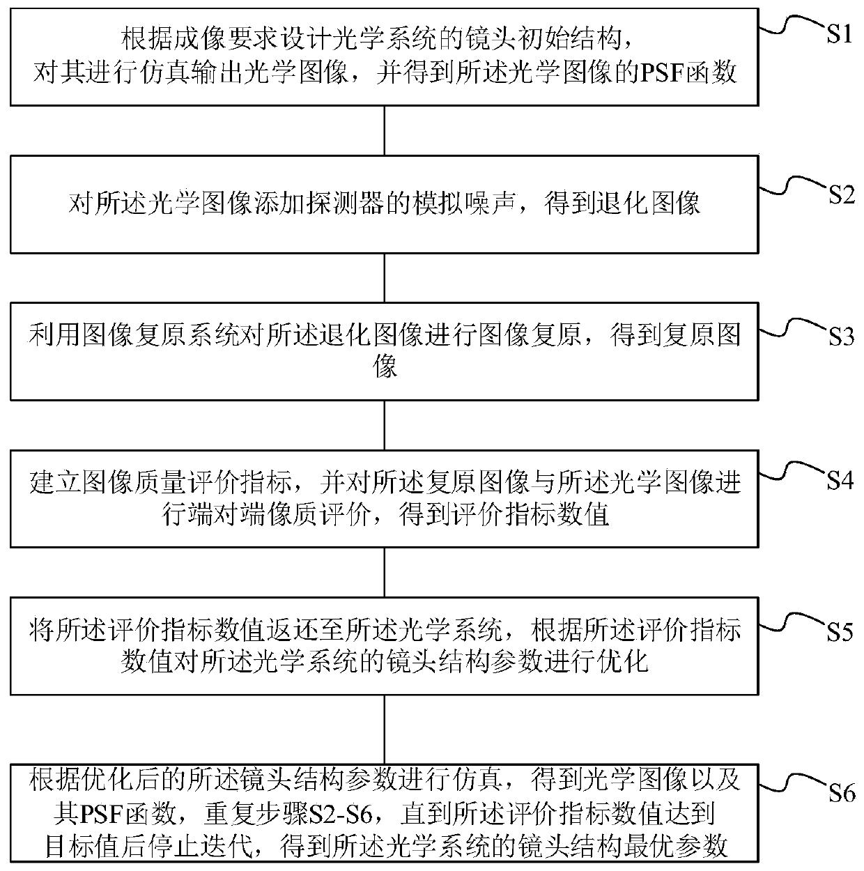
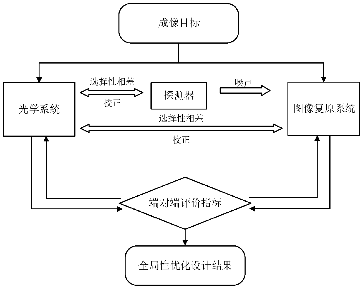
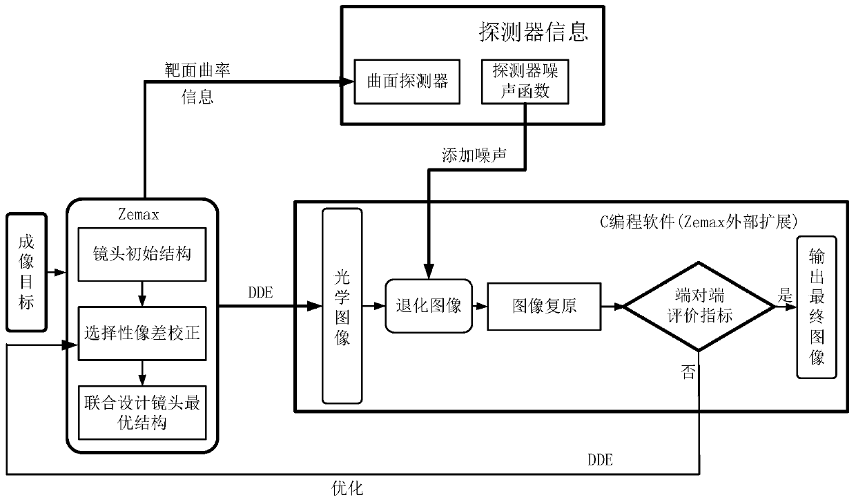
[0042] Please refer to figure 1 , figure 1 It is a flowchart of a global optimization design method for a photoelectric imaging system based on computational imaging provided by an embodiment of the present invention. As shown in the figure, a global optimal design method for a photoelectric imaging system based on computational imaging in this embodiment ,include:

[0043] S1: Design the initial structure of the lens of the optical system according to the imaging requirements, simulate and output the optical image, and obtain the PSF (point spread) function of the optical image;

[0044] S2: adding analog noise of the detector to the optical image to obtain a degraded image;

[0045] S3: Using an image restoration system to perform image restoration on the degraded image to obtain a restored image;

[0046] S4: Establishing an image quality evaluation index, and performing an end-to-end image quality evaluation on the restored image and the optical image, to obtain an eval...

Embodiment 2

[0054] This embodiment is a specific description of the global optimization design method of the photoelectric imaging system based on computational imaging in the first embodiment, and the step S1 includes:

[0055] S11: the initial structure of the lens of the designed optical system is a simple lens optical structure, and according to the Zernike (Zernike) polynomial weighted summation, the PSF function and MTF (modulation transfer) function of the optical image are obtained,

[0056]

[0057]

[0058] In the formula, λ represents the central wavelength of the imaging band of the optical system, D represents the diameter of the exit pupil, and A p Represents the exit pupil area, FT represents Fourier transform, p(x,y) represents the exit pupil function, W(x,y) represents the wavefront optical path difference of each monochromatic geometric aberration;


PUM


Abstract

The invention relates to a global optimization design method of a photoelectric imaging system based on computational imaging. The method comprises the steps of designing a lens initial structure of an optical system according to imaging requirements, imaging the imaging target to obtain an optical image; adding simulation noised to the optical image to obtain degraded images, and using the imagerestoration system to carry out image restoration on the degraded image to obtain a restored image, performing end-to-end image quality evaluation on the restored image and the optical image accordingto the image quality evaluation index, and returning a result to optical system design software, thereby optimizing the whole imaging system to obtain a globally optimized design result. According tothe method, the optical system and the curved surface detector are optimally designed on the basis of correcting the optical phase difference by adopting an image restoration algorithm, so that the design difficulty and complexity of the optical system and the adjustment difficulty of the optical system can be effectively reduced.

Description

technical field [0001] The invention belongs to the technical field of optical system design, and in particular relates to a global optimization design method of a photoelectric imaging system based on computational imaging. Background technique [0002] As a product of the industrial age, traditional photoelectric imaging can well meet the needs of traditional industries. At present, photoelectric imaging equipment generally has the following problems: the use of photoelectric imaging equipment is severely restricted by weather conditions; the optical system is bulky and heavy in photoelectric equipment. Heavy, high processing and assembly costs; defocus, motion blur and lack of depth information are difficult problems for optoelectronic imaging equipment. [0003] The traditional optical system design method is based on the aberration-driven design concept. Because of the diffraction, the point light source passes through the optical system and forms a diffuse spot with a ...

Claims


Application Information

Patent Timeline
IPC IPC(8): G06T7/90G06T5/00G06F17/50
CPCG06T5/002G06T5/007G06T5/001G06T7/90
Inventor 刘飞邵晓鹏冯位欣段景博刘佳维杨思源董磊高苗
Owner XIDIAN UNIV
Why Eureka
Try Eureka