

Photosensitive solder resist material with short exposure time and preparation method thereof
A photosensitive solder mask, exposure time technology, applied in optical mechanical equipment, patterned surface photoengraving process, optics, etc., can solve problems such as restricting the production efficiency of circuit boards, and achieve high hardness, fast light response speed, and adhesion. high effect
- Summary
- Abstract
- Description
- Claims
- Application Information
AI Technical Summary
Problems solved by technology
Method used
Image


Examples
Embodiment 1
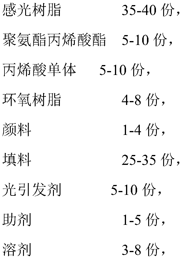
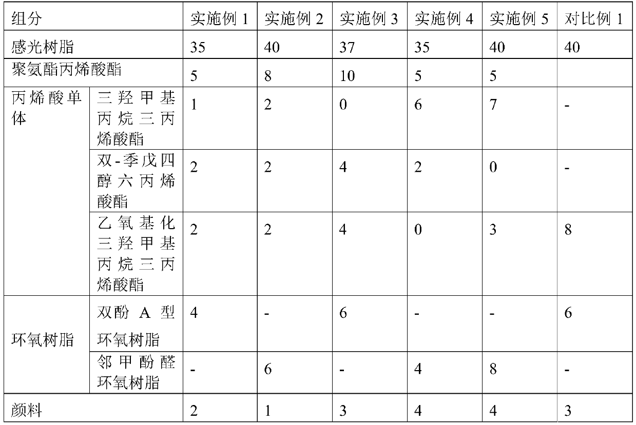
[0039] A prepared photosensitive solder resist material with a short exposure time includes the components shown in Table 1 in parts by weight.
[0040] The preparation method of the photosensitive resin that adopts wherein is: by weight, in reaction container, with 8 parts of acrylic acid, 40 parts of o-cresol novolac epoxy resins, 38 parts of solvents, 0.3 parts of catalysts, 0.3 parts of hydroquinone are heated to After reacting at 100-110°C for 8-12 hours, add 12 parts of acid anhydride and react at 105°C for 4-6 hours, then add 1.5 parts of glycidyl methacrylate and react at 105°C for 4-6 hours. A photosensitive resin with an acid value of 55-65 mgKOH / g and a solid content of 62% was obtained.
[0041] The preparation method of the photosensitive solder resist material with short exposure time comprises the following steps:
[0042] 1) taking photosensitive resin, urethane acrylate, acrylic acid monomer, epoxy resin, photoinitiator, auxiliary agent, solvent, pigment and ...
Embodiment 2
[0047] A photosensitive solder resist material with a short exposure time, comprising the components shown in Table 1 in parts by weight.
[0048] The preparation method of the photosensitive resin that adopts wherein is: by weight, in reaction container, with 12 parts of acrylic acid, 38 parts of o-cresol novolac epoxy resins, 35 parts of solvents, 0.2 parts of catalysts, 0.3 parts of hydroquinone are heated to After reacting at 100-110°C for 8-12 hours, add 12 parts of acid anhydride and react at 105°C for 4-6 hours, then add 2.5 parts of glycidyl methacrylate and react at 105°C for 4-6 hours. A photosensitive resin with an acid value of 55-65 mgKOH / g and a solid content of 65% is obtained.
[0049] The method for preparing a photosensitive solder resist material with a short exposure time is the same as that in Example 1.
Embodiment 3
[0051] A photosensitive solder resist material with a short exposure time, comprising the components shown in Table 1 in parts by weight.
[0052] The preparation method of the photosensitive resin that adopts wherein is: by weight, in reaction vessel, with 15 parts of acrylic acid, 35 parts of o-cresol novolac epoxy resins, 35 parts of solvents, 0.2 parts of catalysts, 0.3 parts of hydroquinone are heated to After reacting at 100-110°C for 8-12 hours, add 12 parts of acid anhydride and react at 105°C for 4-6 hours, then add 2.5 parts of glycidyl methacrylate and react at 105°C for 4-6 hours. A photosensitive resin with an acid value of 55-65 mgKOH / g and a solid content of 65% is obtained.
[0053] The method for preparing a photosensitive solder resist material with a short exposure time is the same as that in Example 1.
PUM
| Property | Measurement | Unit |
|---|---|---|
| acid value | aaaaa | aaaaa |
Abstract
Description
Claims
Application Information