A kind of 5g metal/ceramic composite circuit board and preparation method thereof

A ceramic composite and circuit board technology, which is applied in the direction of circuit substrate materials, printed circuits, printed circuit components, etc., can solve the problems of low bonding strength between copper and ceramics, low yield of laser drilling, and immature drilling technology, etc. , to achieve the effect of being suitable for large-scale industrial production, excellent solderability, and easy control of the production process

Active Publication Date: 2021-03-30
GUANGDONG UNIV OF TECH
View PDF8 Cites 0 Cited by
  • Summary
  • Abstract
  • Description
  • Claims
  • Application Information

AI Technical Summary

Problems solved by technology

[0004] The purpose of the present invention is to overcome the complex production process, immature technology, low bonding strength of copper and ceramic interface, easy peeling off of the ceramic substrate in the prior art, low yield rate of mechanical and laser drilling, heavy workload and difficult drilling technology. Defects or deficiencies such as immaturity, provide a method for preparing a 5G metal / ceramic composite circuit board based on PVD technology

Method used


Image

  • A kind of 5g metal/ceramic composite circuit board and preparation method thereof
  • A kind of 5g metal/ceramic composite circuit board and preparation method thereof
  • A kind of 5g metal/ceramic composite circuit board and preparation method thereof

Examples


Embodiment 1

[0042] This embodiment provides a 5G metal / ceramic composite circuit board, and the specific preparation process is as follows.

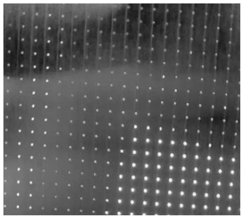
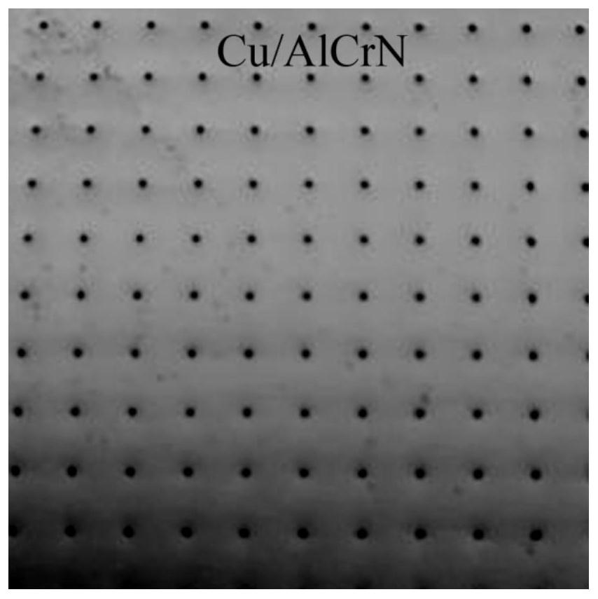
[0043] The 0.3mm thick Al plate purchased in the market is processed on the surface, and a high-density hole array with a diameter of 0.3mm is drilled on its surface (such as figure 1 ), then cleaned, dried, and placed on the multi-target co-deposition preparation platform; adjust the target as needed, for example: copper target and AlCr target, the two targets are arranged alternately (such as Image 6 ); Turn on the mechanical pump and the molecular pump to pump the background vacuum of the vacuum chamber to less than 5.0×10 -3 Pa, feed Ar gas and control the flow rate at 100 sccm, the air pressure is less than 0.2 Pa, the sample temperature is 420 ° C, the negative bias voltage is 300 V, and the bombardment time is 10 min. Turn on the turret and Cu target, keep the sample bias at -80V, keep the sample temperature at 420°C, target current at 120A...

Embodiment 2

[0045] This embodiment provides a 5G metal / ceramic composite circuit board, and the specific preparation process is as follows.

[0046] The 0.3mm thick Al plate purchased in the market is processed on the surface, and a high-density hole array with a diameter of 0.3mm is drilled on its surface (such as figure 1), and then cleaned, dried, and placed on the multi-target co-deposition preparation platform; adjust the target as needed, for example: copper target and Al target, the two targets are arranged alternately; turn on the mechanical pump and molecular pump to reduce the background of the vacuum chamber Vacuum to less than 5.0×10 -3 Pa, feed Ar gas and control the flow rate at 100 sccm, the air pressure is less than 0.2 Pa, the sample temperature is 420 ° C, the negative bias voltage is 300 V, and the bombardment time is 10 min. Turn on the turret and Cu target, keep the sample bias at -80V, keep the sample temperature at 420°C, target current at 120A, deposit for 5min, a...

Embodiment 3

[0048] This embodiment provides a 5G metal / ceramic composite circuit board, and the specific preparation process is as follows.

[0049] The 0.3mm thick Al plate purchased in the market is processed on the surface, and a high-density hole array with a diameter of 0.35mm is drilled on its surface (such as Figure 4 ), and then cleaned, dried, and placed on the multi-target co-deposition preparation platform; adjust the target as needed, for example: copper target and Cr target, the two targets are arranged alternately; turn on the mechanical pump and molecular pump to reduce the background of the vacuum chamber Vacuum to less than 5.0×10 -3 Pa, feed Ar gas and control the flow rate at 100 sccm, the air pressure is less than 0.2 Pa, the sample temperature is 420 ° C, the negative bias voltage is 300 V, and the bombardment time is 10 min. Turn on the turret and Cu target, keep the sample bias at -80V, keep the sample temperature at 420°C, target current at 120A, deposit for 5min...


PUM

PropertyMeasurementUnit
thicknessaaaaaaaaaa
thicknessaaaaaaaaaa
thicknessaaaaaaaaaa

Abstract

The present invention relates to a 5G metal / ceramic composite circuit board and a preparation method therefor. The preparation method comprises the following steps: alternately depositing metal layers and ceramic layers on a metal substrate with a preset hole by using a PVD technique, to obtain a 5G metal / ceramic composite circuit board. According to the preparation method for a metal / ceramic composite circuit board of the present invention, the difficulties of a conventional technique (a ceramic / metal thermal diffusion bonding method) for a metal / ceramic composite circuit board, such as being complex, low in yield, high in price, low in efficiency and undeveloped in terms of technique, are avoided. In addition, according to the preparation method of the present invention, a metal substrate with a hole is selected, such that the problems of laser / mechanical composite drilling of a ceramic substrate whereby same is low in yield, large in terms of workload, and undeveloped in terms of drilling technique, are solved. In the present invention, a combined technique of a physical vapor deposition technique and a template technique is used to deposit the metal layer and the ceramic layer, all the layers in the obtained metal / ceramic composite circuit board are high in terms of bonding strength and are not prone to stripping, and the technique is simple.

Description

technical field [0001] The invention belongs to the technical field of circuit boards, and in particular relates to a 5G metal / ceramic composite circuit board and a preparation method thereof. Background technique [0002] The transmission rate of 5G is as high as 10Gbps, the capacity is 1000 times higher than that of 4G, the end-to-end extension is 10 times smaller, and can reach the millisecond level, the spectral efficiency is 5-10 times higher than that of 4G, and the frequency is higher. Based on the above characteristics, 5G technology is defined by the Ministry of Industry and Information Technology as a revolution, and countries all over the world are grabbing the highest point. Among them, ceramic substrate is one of the key technologies that limit the development of 5G technology. [0003] The mainstream preparation technology of ceramic substrate refers to the special process board in which the copper foil is directly bonded to the surface of the ceramic substrat...

Claims


Application Information

Patent Timeline
Patent Type & Authority Patents(China)
IPC IPC(8): C23C14/34C23C14/16C23C14/06H05K1/03H05K1/05
CPCC23C14/0641C23C14/165C23C14/3464H05K1/0306H05K1/05
Inventor 陈汪林李炳新王成勇颜安
Owner GUANGDONG UNIV OF TECH
Why Eureka
Try Eureka