Growth method of LED epitaxial structure

A growth method and epitaxial structure technology, applied in gaseous chemical plating, coating, electrical components and other directions, can solve the problems of low growth quality of quantum wells and low radiation recombination efficiency of quantum wells, so as to improve luminous efficiency and reduce luminescence. Attenuation effect, the effect of improving product yield

Active Publication Date: 2019-12-31
XIANGNENG HUALEI OPTOELECTRONICS
View PDF7 Cites 6 Cited by
  • Summary
  • Abstract
  • Description
  • Claims
  • Application Information

AI Technical Summary

Problems solved by technology

[0005] The invention solves the problems of low quantum well growth quality and low quantum well radiation recombination efficiency existing in the existing LED epitaxial growth method by adopting a new multi-quantum well layer growth method, thereby improving the luminous efficiency of the LED and reducing the number of epitaxial wafers. Warpage, improve product yield

Method used


Image

  • Growth method of LED epitaxial structure
  • Growth method of LED epitaxial structure
  • Growth method of LED epitaxial structure

Examples


Embodiment 1

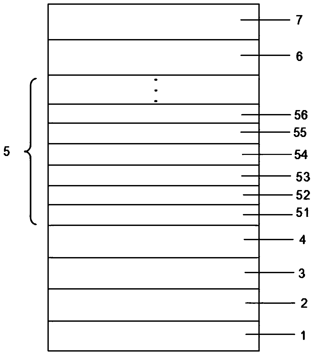
[0041] This embodiment adopts the LED epitaxial structure growth method provided by the present invention, adopts MOCVD to grow GaN-based LED epitaxial wafers, and uses high-purity H 2 or high purity N 2 or high purity H 2 and high purity N 2 The mixed gas as the carrier gas, high-purity NH 3 As the N source, the metal-organic source trimethylgallium (TMGa) is used as the gallium source, trimethylindium (TMIn) is used as the indium source, and the N-type dopant is silane (SiH 4 ), trimethylaluminum (TMAl) as the aluminum source, and the P-type dopant as magnesium dicene (CP 2 Mg), the reaction pressure is between 70mbar and 900mbar. The specific growth method is as follows (for the epitaxial structure, please refer to figure 1 ):

[0042] A method for growing an LED epitaxial structure, which sequentially includes: processing a substrate 1, growing a low-temperature buffer layer GaN2, growing an undoped GaN layer 3, growing a Si-doped N-type GaN layer 4, growing a multi-...

Embodiment 2

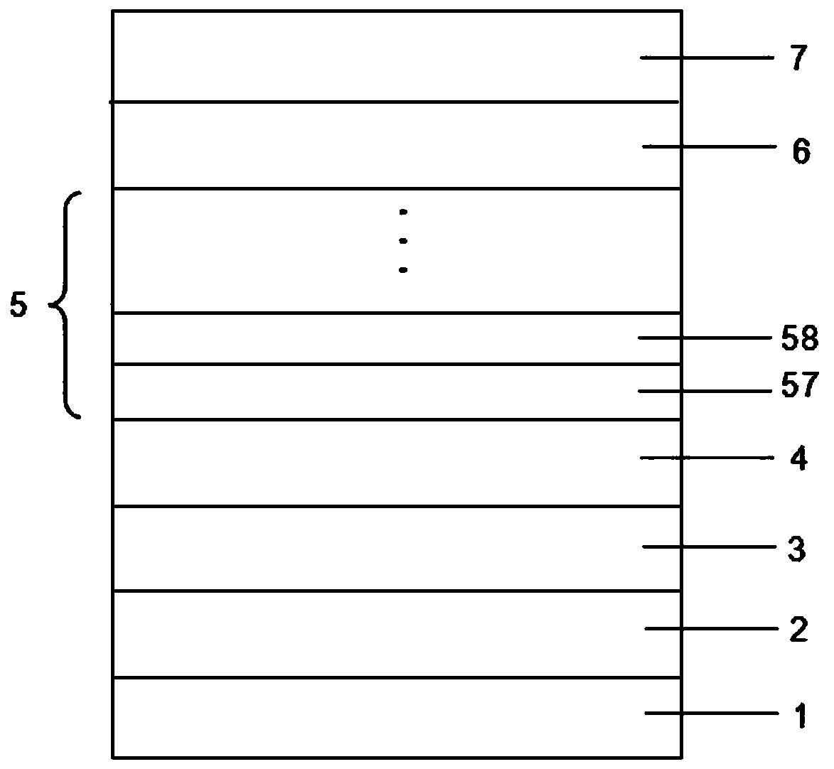
[0073] Comparative examples are provided below, that is, the growth method of the traditional LED epitaxial structure (for the epitaxial structure, please refer to figure 2 ).

[0074] Step 1: At a temperature of 1000-1100°C and a reaction chamber pressure of 100-300mbar, feed 100-130L / min of H 2 Under the conditions, process the sapphire substrate for 5-10 minutes.

[0075] Step 2: growing a low-temperature GaN buffer layer, and forming irregular small islands in the low-temperature GaN buffer layer 2 .

[0076] Specifically, the step 2 is further as follows:

[0077] At a temperature of 500-600°C and a reaction chamber pressure of 300-600mbar, 10000-20000sccm of NH is introduced 3 , 50-100sccm TMGa, 100-130L / min H 2 Under the condition of , the low-temperature buffer layer GaN2 is grown on the sapphire substrate 1, and the thickness of the low-temperature GaN buffer layer 2 is 20-40nm;

[0078] At a temperature of 1000-1100°C and a reaction chamber pressure of 300-600m...


PUM

PropertyMeasurementUnit
thicknessaaaaaaaaaa
thicknessaaaaaaaaaa
thicknessaaaaaaaaaa

Abstract

The invention discloses a growth method of an LED epitaxial structure. The method comprises the successive steps of treating a substrate, growing a low-temperature buffer layer GaN, growing a doping-free GaN layer, growing a Si-doped N-type GaN layer, growing a multi-quantum well layer, growing a AlGaN electronic blocking layer, growing a Mg-doped P-typed GaN layer and performing cooling. The process of growing the multi-quantum well layer comprises the successive steps of growing a high-temperature InGaN well layer, growing a low-temperature GaN base layer, growing a high-Al-component gradualchange AlN layer, growing a Si-doped low-temperature InGaN well layer, growing a high-temperature GaN base layer and growing a low-Al-component gradual change AlN layer. According to the method, theproblems are solved that for an existing LED epitaxial growth method, the growth quality of the quantum well is low, and the radiation recombination efficiency of the quantum well is low. The luminescence efficiency of an LED is improved accordingly, warping of an epitaxial slice is reduced, and forward voltage of the LED is lowered.

Description

technical field [0001] The invention belongs to the technical field of LEDs, and in particular relates to a method for growing an LED epitaxial structure. Background technique [0002] A light-emitting diode (Light-EmittingDiode, LED) is a semiconductor electronic device that converts electrical energy into light energy. When the LED has current flowing, the electrons and holes in the LED recombine in its multiple quantum wells to emit monochromatic light. As a new type of high-efficiency, environmentally friendly and green solid-state lighting source, LED has the advantages of low voltage, low energy consumption, small size, light weight, long life, high reliability and rich colors. At present, the scale of domestic production of LEDs is gradually expanding, but LEDs still have the problem of low luminous efficiency, which affects the energy-saving effect of LEDs. [0003] The quality of LED epitaxial InGaN / GaN multi-quantum wells prepared by the existing LED multi-quantu...

Claims


Application Information

Patent Timeline
Patent Type & Authority Applications(China)
IPC IPC(8): C23C16/44C23C16/30H01L33/00H01L33/06H01L33/32
CPCC23C16/303C23C16/44H01L33/007H01L33/06H01L33/325
Inventor 徐平胡耀武王杰黄胜蓝
Owner XIANGNENG HUALEI OPTOELECTRONICS
Why Eureka
Try Eureka