

Manufacturing method of surface embossment grating structure
A technology of grating structure and manufacturing method, which is applied in the direction of diffraction grating, optics, optical elements, etc., can solve the problems of laser direct writing that cannot accurately control the contour depth, low work efficiency, contour depth error, etc., to reduce the exposure and development process, Increased productivity and wide-ranging effects
- Summary
- Abstract
- Description
- Claims
- Application Information
AI Technical Summary
Problems solved by technology
Method used
Image

Examples
Embodiment Construction
[0046] The present invention will be further described below in conjunction with the accompanying drawings and embodiments.
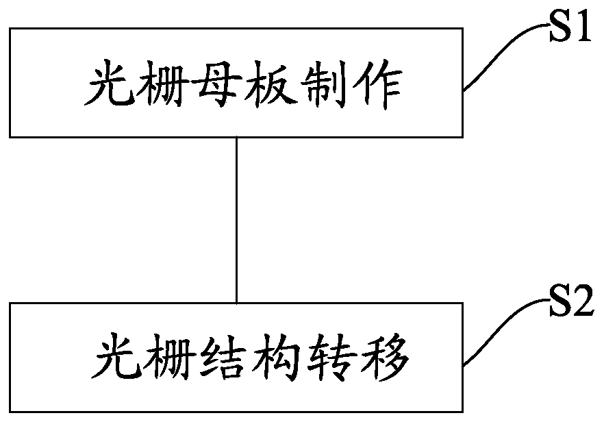
[0047] see Figure 1-2 , the invention discloses a method for manufacturing a surface relief grating structure, comprising the following steps:
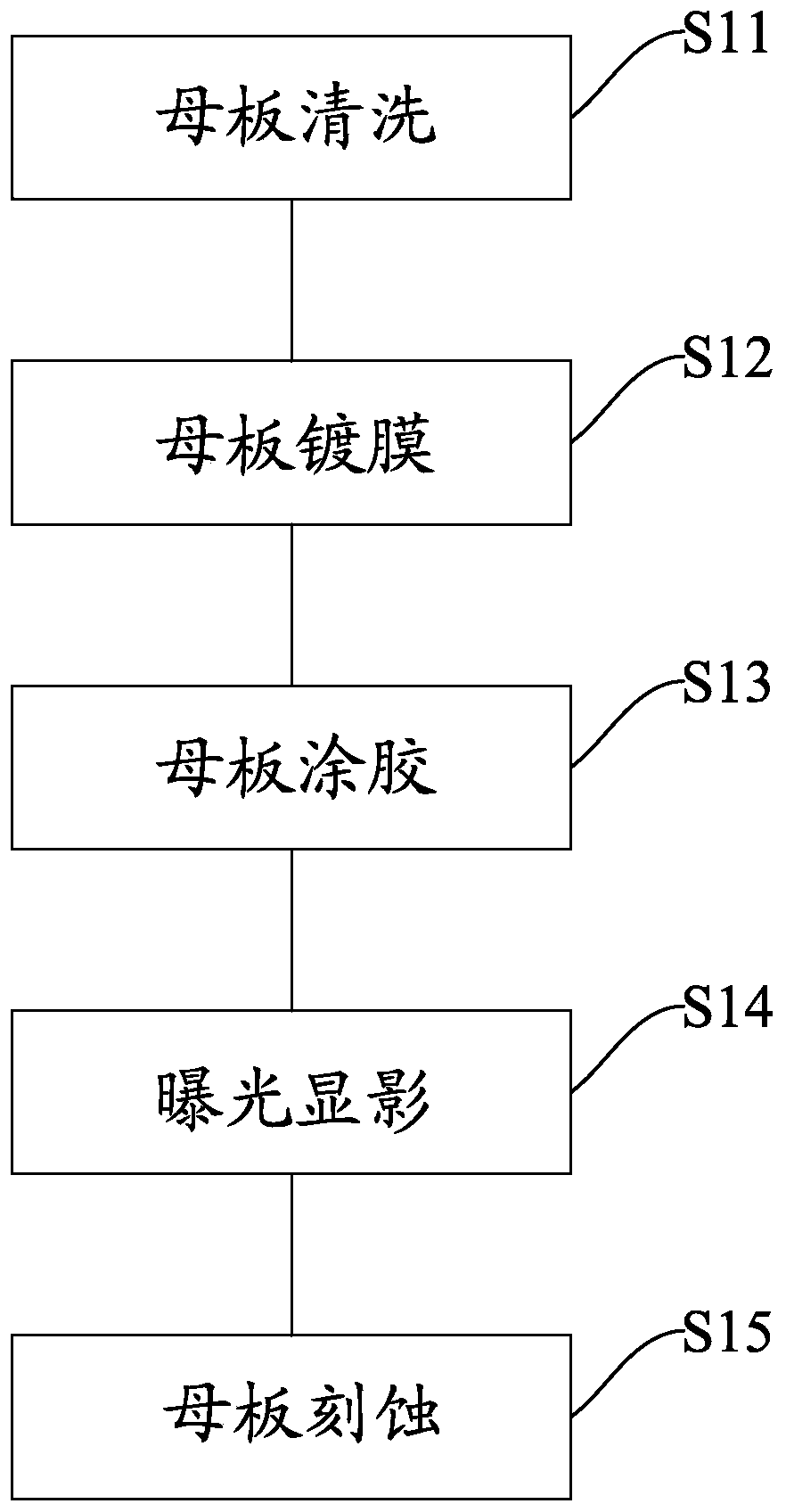
[0048] S1, making the grating master, including the following steps:
[0049] S11. Motherboard cleaning: provide the substrate substrate, place the substrate substrate in cleaning equipment, soak it in absolute ethanol and acetone, remove residual organic matter, and then use a large amount of deionized water to rinse and dry; substrate The substrate is generally made of silicon or plastic.
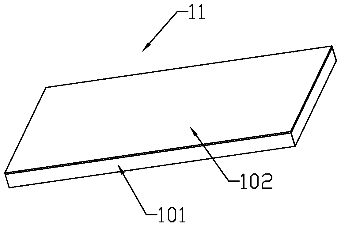
[0050]S12, Motherboard Coating: On the surface of the substrate 101, a metal film layer 102 with an etching rate different from that of the substrate 101 is coated to obtain the first grating motherboard 11, such as image 3 shown;
[0051] Specifically, a metal chromium layer is formed on the base material 101 by mag...
PUM
| Property | Measurement | Unit |
|---|---|---|
| Width | aaaaa | aaaaa |
Abstract
Description
Claims
Application Information